ANSYS LUMERICAL

Lumerical FDTD: broadband analysis of nanophotonic devices of arbitrary shape

Solves Maxwell’s equations numerically by the finite-difference time-domain method. Because no approximation restricts the direction or angle of propagation, three-dimensional behavior including back reflection and multiple reflections is handled directly.
3D FDTDGPUGDSIIJapanese-language support

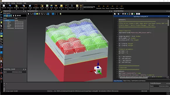
The Lumerical FDTD analysis screen, with the microlens structure of a CMOS image sensor shown in the layout view beside the script editor

What FDTD is

Solving Maxwell’s equations directly, in the time domain

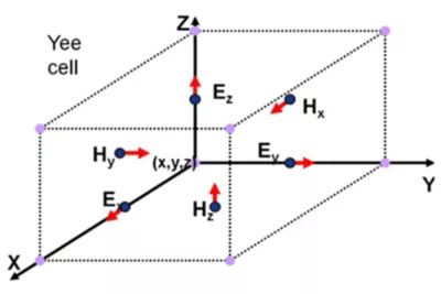
The analysis volume is divided into a grid, and the electric and magnetic fields are updated alternately at each time step. It applies to a wide range of geometries and can model material dispersion and anisotropy, which makes it the most generally applicable method for analyzing nanophotonic devices.

Because the calculation is in the time domain, launching a single broadband pulse and taking its Fourier transform gives the response across the whole wavelength range from one run. That matters when you are designing resonator Q factors or filter transmission spectra.

The cost, though, grows with the number of cells multiplied by the number of time steps. Where the analysis region is large compared with the wavelength, or a fine mesh, a long decay time or dispersive materials are needed, run time and memory use grow accordingly. Depending on the problem, it is worth choosing between FDTD and the RCWA and STACK solvers included in the same Lumerical FDTD product, or the FDE, EME and varFDTD solvers in the separate Lumerical MODE product.

The Yee cell used for spatial discretization in the FDTD method, showing electric field components on the edges and magnetic field components on the faces of an orthogonal grid

What FDTD gives you

Three things FDTD gives you

01

Full-wave analysis

Solves Maxwell’s equations numerically in the time domain, with no approximation restricting the direction or angle of propagation. Accuracy depends on the mesh, the time step, the material model and the boundary conditions. Back scattering, multiple reflections and diffraction in every direction are included directly.

02

Broadband

Using a broadband pulse with frequency-domain monitors, the response at many wavelengths can usually be obtained from a single simulation. Cases such as oblique incidence on a periodic structure may need BFAST or a wavelength and angle sweep.

03

GPU execution

From 2023 R2 onwards, 3D FDTD analysis on supported NVIDIA GPUs is available. Single-GPU, multi-GPU and distributed execution in supported environments are possible, but there are constraints on material models, boundary conditions, GPU specification, licensing and the number of SMs available. Setup changes between releases, so please check the requirements for the version you are using.

FDTD analysis of a negative-index medium, showing an incident beam refracting the opposite way to normal at the interface

Where it fits

Where FDTD fits, and where it does not

Its generality has a cost, and for some problems another method solves faster and more accurately. The following is a guide to choosing.

Use FDTD when

  • the characteristic dimensions of the structure are comparable with the wavelength or smaller
  • the geometry is arbitrary, with neither periodicity nor uniformity along the propagation direction to assume
  • you need spectral characteristics over a wide wavelength range in one go
  • back scattering and multiple reflections have to be included in the evaluation
  • you need resonator Q factors, filter response, or grating coupler efficiency
  • you need far-field patterns or radiation efficiency

Consider another method

  • The structure is strictly periodic and only diffraction efficiency is needed → RCWA
  • You need the modes of a waveguide → MODE (FDE) or Multiphysics (FEEM)
  • You are analyzing long-distance waveguide propagation, or a structure with a clear dominant propagation direction → MODE (EME / varFDTD)
  • Only the reflectance spectrum of a multilayer stack is needed → STACK
  • You are handling complex curved surfaces, or a geometry where an unstructured mesh helps → DGTD
  • You want to see the whole PIC or link performance → INTERCONNECT

For periodic structures RCWA is generally faster, while FDTD suits non-periodic structures and more general analysis.

Typical applications

Where it is used

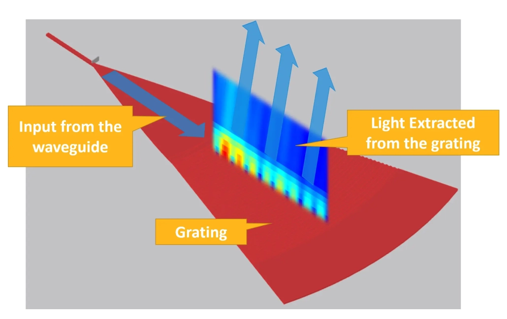
FDTD analysis of a grating coupler

Silicon Photonics

Characterizing grating couplers, directional couplers, ring resonators and MMIs

View solutions

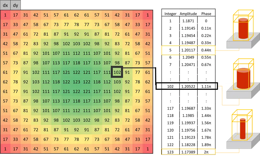
Phase map of a metalens

Metalenses and metasurfaces

Verifying the response of a single meta-atom, and checking local focusing performance

View solutions

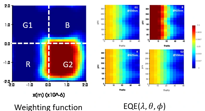
CMOS image sensor characterization results, showing the Bayer weighting functions and the angular and spectral dependence of external quantum efficiency for each color pixel

Image sensors

Optical efficiency and color crosstalk of pixel structures including microlenses and color filters

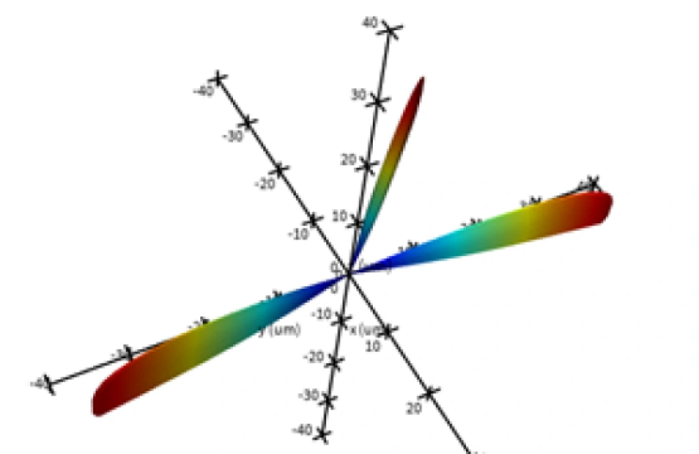
FDTD analysis of a LiDAR antenna, showing the three-dimensional far-field radiation pattern in angular coordinates

LiDAR and optical sensing

Radiation patterns of antenna elements, and OPA element design

View solutions

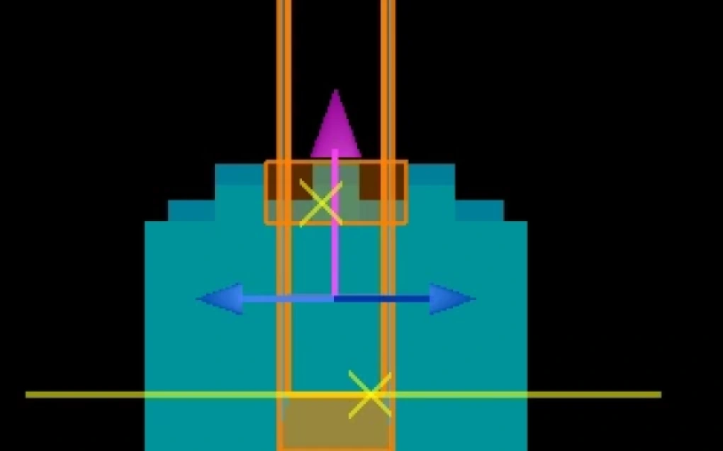
FDTD model of a resonant biosensor grating, showing the grating cross-section with the source and the reflection and transmission monitors in place

Biosensors

Maximizing the sensitivity of SPR structures and waveguide sensors

View solutions

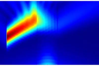
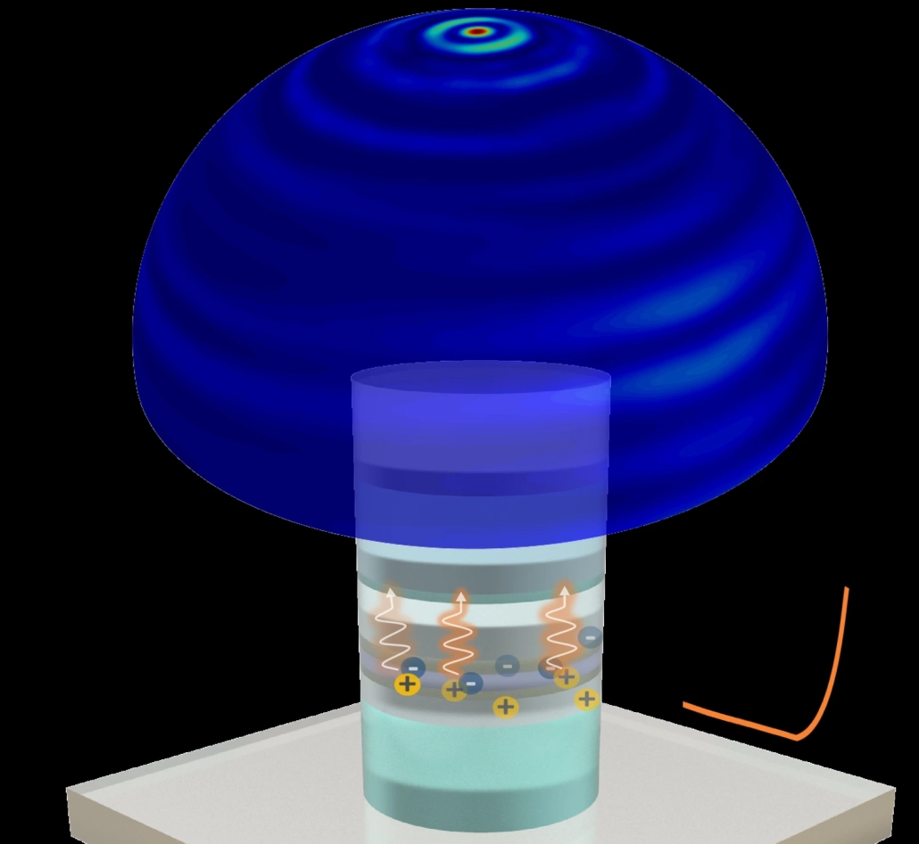
FDTD analysis of a micro-LED, showing the device structure and the far-field intensity distribution it radiates

Light-emitting devices

Light extraction efficiency of LEDs and OLEDs, and emission control in microcavities

Inputs and outputs

What you provide, and what you get

For the structure, materials, source and boundary conditions you set, it returns the electromagnetic field distribution, transmission, reflection and absorption spectra, S-parameters, far fields and more.

INPUT

What you need to prepare

GeometryBuilt-in primitives, GDSII import, STL and STEP import, parametric generation by script
MaterialFitting to measured n and k data, dispersion models, anisotropic materials, nonlinear materials
Light sourcePlane wave, Gaussian, mode source, dipole, TFSF, imported field
Boundary conditionsPML, periodic, Bloch, symmetric and antisymmetric, metal
MeshAutomatic generation, plus region-specific mesh refinement and conformal mesh
MonitorsFrequency domain, time domain, far-field projection, movie output

FDTD

Finite-difference time-domain method

OUTPUT

What you get

SpectrumWavelength dependence of transmittance, reflectance and absorptance
S-parametersS-parameters including amplitude and phase between ports. These can be used for an INTERCONNECT circuit model or to create a CML (generating a compiled CML requires CML Compiler)
Electromagnetic field distributionE and H distributions on a cross-section or through a volume, Poynting vector, intensity distribution
Far fieldRadiation pattern, directivity, and focusing efficiency against numerical aperture
Resonant characteristicsResonant wavelength, Q factor, mode volume
Data for handoverBeam-like fields from a frequency-domain monitor are passed to OpticStudio in ZBF format. A strongly confined near field needs a far-field transformation or similar first. Optical absorption distributions are passed to CHARGE and HEAT

Analysis workflow

How it works in practice

Skip the convergence check and you cannot judge whether a result is sound. Step 03 is where most of your time should go.

01

Define the structure and materials

Import from GDSII or CAD, or define the dimensions as parameters. At the same time, check the fitting error of the material model against measured data over the wavelength range of interest. Get this wrong and everything after it is wrong.

02

Set up sources, boundaries and monitors

Where symmetry can be used, symmetric and antisymmetric boundaries cut the computation substantially.

03

Check convergence

Vary the mesh, the simulation time, the number of PML layers and the size of the analysis region, and confirm that the result stops moving.

04

Run parameter sweeps and optimization

Vary the dimensions to map out the design space. Parallel execution on HPC and in the cloud is supported.

05

Hand the results on

S-parameters to INTERCONNECT, absorption distributions to CHARGE and HEAT, beams to Zemax.

Frequently asked questions

Questions we are often asked about FDTD

Questions we are often asked before adoption.

Where the structure is periodic and you are evaluating diffraction efficiency or phase by wavelength, angle and polarization, use RCWA. Where finite-size effects, local defects, or arbitrary geometry with no periodicity are involved, use FDTD. In metasurface design you can generate the meta-atom library with RCWA and, where needed, verify local and finite-size effects with FDTD.

Vary the mesh accuracy, mesh overrides, the number of PML layers and the distance between the structure and the PML, and confirm that the result you care about has converged sufficiently. Also confirm that the simulation time and the auto shutoff setting are not affecting the result.

Start with the material model and its fitting, the mesh, and the boundary conditions including the PML. If you cannot identify the cause, simplify the model and narrow down where the problem is by inspecting the field distribution.

Yes. FDTD can use a supported NVIDIA GPU to accelerate 3D simulations. There are version-specific requirements and limitations on which GPUs, licenses and features are available, so please talk to us before you buy.

It depends on the scale of the analysis, but RAM capacity and memory bandwidth matter most. For large analyses we recommend a CPU environment with ample RAM and high memory bandwidth, plus a supported GPU where appropriate. We will advise on a configuration to match the analysis you have in mind.

Japanese-language support and training

We can advise on analysis setup, convergence, and how to choose boundary conditions. Hands-on training working directly in FDTD and MODE is also available.

Helpful to know before we talk

  • Target wavelengths and materials
  • Device structure and approximate dimensions
  • The characteristics you want to evaluate, and your target values
  • Whether you already have simulation data or measurements
  • Your expected schedule

You do not need to share everything. Whatever you are able to tell us is enough.

Try it on the structure you actually need to solve

The demo uses a structure close to your own. We can also give you an idea of the computational scale and the time it takes.