
Home/Products/Photonica

PHOTONICA / WORKFLOW PLATFORM

Connecting optical and photonics design from analysis through to system and implementation

Photonica is the optical and photonics design workflow platform developed by LightBridge. An intuitive interface and Python scripting organize the design workflow, bringing in analysis results and design data and carrying them from integration with external design and simulation environments through to layout and manufacturing data.

One connected design workflow

Design and analysis

Design conditions, analysis results and parameters in one place

Integration and visualization

Connections to external simulation environments, and a visible workflow

Implementation and manufacturing

From layout generation to handover of prototype and manufacturing data
The thinking behind the platform

Bringing fragmented design and analysis into one workflow

In optical and photonics design, analysis results, design parameters, and geometry and layout data are spread across several tools and stages, so passing data between them and keeping it up to date tends to be manual work. Photonica connects that design and analysis data and organizes visualization, parameter expansion, geometry and layout generation, and external tool integration into a single workflow. It is a platform for building a design process in which analysis results feed back into the design and can be compared and updated repeatedly.

Why integrate the workflow

Less effort moving back and forth between design and analysis

01

Visualization

See design conditions, structure and layout visually

02

Interoperability

Data exchange with design and simulation environments, organized as a workflow

03

Compare and update

Bring analysis results in, then compare and update design options

What the platform is made of

The foundation you build a workflow on

An intuitive interface

An interface you can work in while watching the state of the workflow and its results.

Python scripting

Automation of design procedures, and workflows written so they can be run again.

Simulation and library data

Put analysis results and library data to work in the design process.

Handling parameters and geometry

Management of design parameters, and generation and manipulation of geometry.

Visualization

Build checks on design data and results into the process itself.

Large-scale layout generation

Where the workflow supports it, large-scale design and layout generation can be handled.

External tool integration

Exchange data with external design and simulation environments, joining several stages into one workflow.

Manufacturing data output

Where the workflow supports it, manufacturing data such as GDS is written out.

Coverage differs by workflow product. Please see the individual product pages.

PHOTONICA PRODUCTS

Workflow products on the platform

Workflow products for individual fields will be rolled out on the Photonica platform. The first of them is below.

Scheduled for release in September 2026

Photonica Metalens Engine

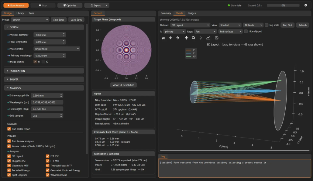
It takes in the phase and transmittance library generated in Ansys Lumerical and handles phase design, phase-to-geometry mapping, placement and layout generation for large metalenses, output of GDSII, ROI GDS and the placement database, and system evaluation and optimization in Zemax OpticStudio. Verified design scales and measured results are given on the Photonica Metalens Engine.

View the product page

Post-placement verification view in Photonica Metalens Engine, with maps and graphs for achieved phase, transmittance, phase error, library usage and pillar cross-section

Further workflow products will be added here as they become available.

Where it sits in the workflow

Analysis, design and implementation in one workflow

ANALYSIS

Analysis and simulation

Device characteristics and analysis results obtained in Ansys Lumerical and elsewhere are brought into Photonica and put to work in the design workflow.

DESIGN & SYSTEM

Design and system integration

Depending on the workflow, data is exchanged with design and system environments such as Zemax OpticStudio, joining device-level and system-level design.

IMPLEMENTATION

On to implementation

Design data such as layouts and GDS is carried through to manufacturing, implementation and the downstream stages.

Try Photonica on a real design

Tell us the design target, workflow or problem you have in mind and we will put together a demo to suit it.