ANSYS LUMERICAL

Lumerical INTERCONNECT: analysing photonic circuits and the link as a whole

Individual device characteristics are connected as compact models to evaluate the performance of a photonic circuit and of the link as a whole. You can see straight away how a change to a device design affects system performance.
PIC designLink analysisEye diagrams

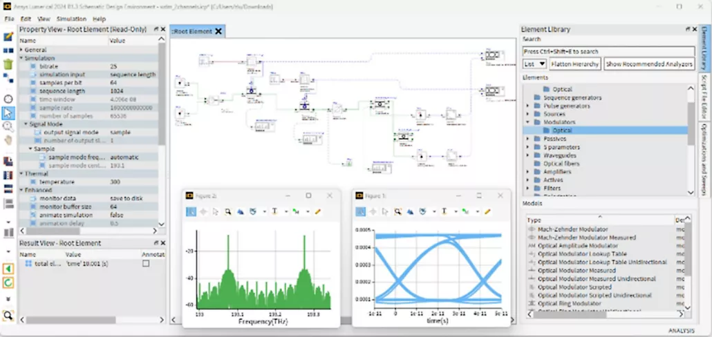
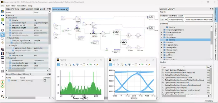
An analysis view in Lumerical INTERCONNECT, showing the photonic circuit schematic alongside spectrum and eye diagram results in the same environment

Overview

Evaluating a collection of elements as a system

A device that performs well on its own will not necessarily meet specification once it is built into a circuit. Accumulated insertion loss, multiple interference from reflections, variation between elements — these only become visible when the system is solved as a whole.

S-parameters obtained from FDTD or MODE are imported as compact models and connected in schematic form. Both time-domain and frequency-domain analysis are supported.

Simultaneous electro-optical analysis is also supported, so a transmit and receive system can be evaluated including basic electrical circuit elements. To solve as far as transistor-level drivers and TIAs, EDA integration such as co-simulation with Cadence Spectre is used.

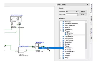
A Lumerical INTERCONNECT view, showing components of a photonic circuit being selected from the element library and placed on the schematic

The advantages of INTERCONNECT

What connecting the levels buys you

01

Connecting the levels

Data from device analysis or from measurement can be carried into the circuit analysis as compact models.

02

Time and frequency

Both eye diagrams and frequency response are covered.

03

Variation

Where a statistical model exists, Monte Carlo analysis gives you yield; where process corners are defined, corner analysis gives you the range of performance.

A circuit analysis view in Lumerical INTERCONNECT, showing the schematic of the complete link together with spectrum and eye diagram results

Where it fits

Where it fits, and where it does not

There are cases another method will solve faster and more accurately. The following is a guide to choosing.

Use INTERCONNECT

  • Accumulating insertion loss and crosstalk across a whole PIC
  • Evaluating eye opening and BER for an optical link
  • Examining inter-channel interference in a WDM system
  • Designing a transmit and receive system including modulators and photodetectors
  • Seeing how a change in device specification affects link performance

Consider another method

  • The electromagnetic field of a single device → FDTD or MODE
  • Generating compact models → CML Compiler
  • Designing in the same schematic as the electronic circuit → Cadence Virtuoso (co-simulation of Spectre with INTERCONNECT, or a Photonic Verilog-A model)

How single-device analysis and integrated circuit-level analysis divide the work.

Typical applications

Where it is used

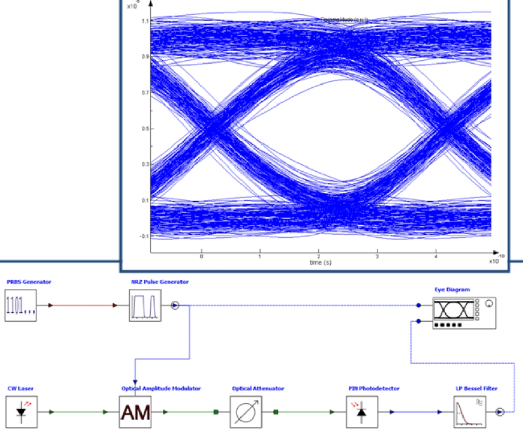
System analysis of an optical transceiver in INTERCONNECT, showing the transmit and receive link schematic and the eye diagram of the received signal

Optical transceivers and CPO

Eye opening and BER for the transmit and receive link

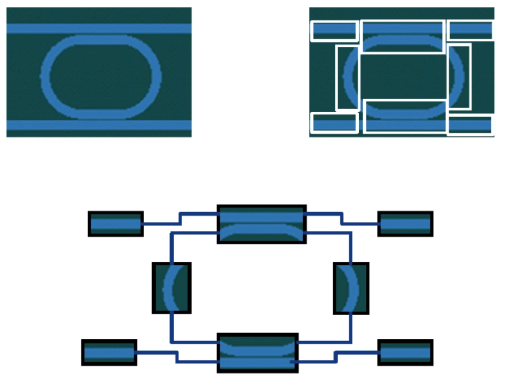
Comparison of simulation approaches for a ring resonator: from a full FDTD analysis to a partitioned workflow that separates the coupling region from the waveguide and reassembles them in INTERCONNECT.

Silicon photonics

Accumulating performance across a whole PIC

View the solution

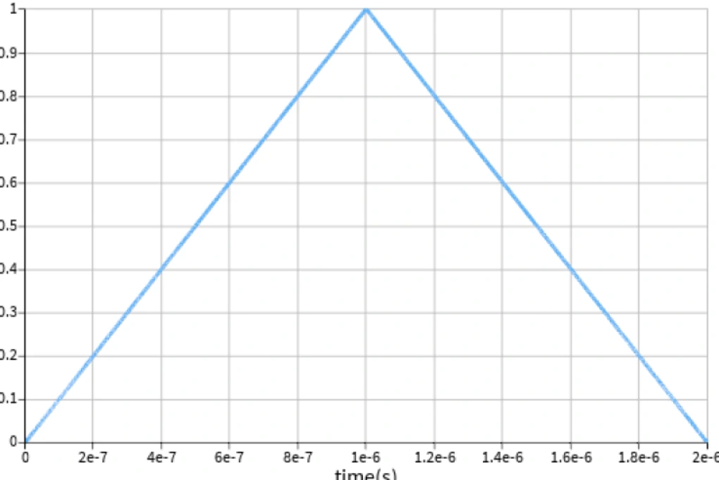
Frequency modulation waveform of the source in an FMCW LiDAR, showing the frequency swept as a triangular wave over time

LiDAR

Range resolution and ranging distance for an FMCW link

View the solution

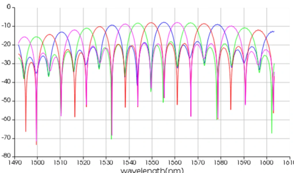
Wavelength response of a WDM circuit, showing the transmission spectra of several channels from 1490 to 1610 nm

WDM systems

Channel allocation and crosstalk

Inputs and outputs

What you supply, and what you get back

For the circuit configuration and signal conditions you set, transmission characteristics and signal quality are returned.

INPUT

What you need to prepare

Compact modelsS-parameters, CML libraries, built-in element models
Circuit configurationHow the elements are connected
Signal sourceModulation format, bit rate, source characteristics
Analysis settingsTime domain or frequency domain

INTERCONNECT

Circuit simulation

OUTPUT

What you get back

Eye diagramOpening, jitter, extinction ratio
BERBit error rate, Q factor, eye opening ratio
Frequency responseTransfer function, group delay
SpectrumSignal power, noise power and OSNR for each channel

Analysis workflow

How the work actually proceeds

Too low a sample rate cannot represent the bandwidth of the time waveform; too short a time window cannot resolve narrow spectral features. Settings chosen to match the purpose of the analysis translate directly into the accuracy of the result.

01

Load the compact model library

Install the .cml received from the foundry into Design Kits.

02

Build the schematic

Place elements from the Element Library or a Design Kit to assemble the circuit. Where needed, import S-parameters or data from measurement or device analysis, in the format the element model expects.

03

Set the solver and the signal conditions

Choose between TSM (suited to closed loops), TBM (suited to open loops) and SPS (frequency domain). Sample rate and time window are time-domain settings, for TSM and TBM.

04

Place the instruments and run

Use the Optical Network Analyzer for transmission, group delay and dispersion, and the Eye Diagram for BER and jitter.

05

Sweep, optimise and evaluate yield

Beyond parameter sweeps and optimisation, where a statistical model is available Monte Carlo analysis gives you the yield against manufacturing variation. Where the CML defines process corners, corner analysis shows the range of performance for each condition.

EDA integration

Using it alongside an EDA environment: Photonic Verilog-A

Photonic Verilog-A is part of the INTERCONNECT and CML Compiler workflow. Models for an electronic design automation (EDA) environment are generated from the same source data, so a photonic circuit can be handled in the same schematic as the electronic circuit.

Choosing between this and INTERCONNECT

INTERCONNECT is for analysing photonic circuits; Photonic Verilog-A is for co-simulation of electronic and photonic circuits inside an EDA environment. Both can draw on the same model source data.

Generating models with CML Compiler

CML Compiler generates the Photonic Verilog-A models, building a library from the source data for each element and distributing it for the EDA environment.

Cadence Virtuoso / Spectre

The classic workflow. Load the generated models and symbols into Virtuoso, and take the electronic and photonic circuits through design, simulation and layout in the same schematic.

Synopsys OptoCompiler

Supports co-simulation of electronic and photonic circuits using OptoCompiler with PrimeSim SPICE / PrimeSim HSPICE. For supported versions and operating environments, please see the latest system requirements.

There is no license specific to Photonic Verilog-A. On the Ansys side it is available under an INTERCONNECT or Enterprise license, and generating the models requires a CML Compiler license. A license for the EDA tool itself is required separately.

INTERCONNECT compact models and Photonic Verilog-A models pass signals and information in fundamentally different ways, so they cannot be connected optically within the same circuit.

Frequently asked questions

Questions we are often asked about INTERCONNECT

The questions we are most often asked before adoption.

S-parameters extracted in FDTD can be imported as an S-parameter element or a compact model in INTERCONNECT. The modes, ports and frequency or wavelength range must be kept consistent between the two.

Yes. INTERCONNECT on its own can analyse electro-optical circuits that include basic electrical circuit elements. For detailed simultaneous analysis of electronic and photonic circuits including transistor-level drivers and TIAs, EDA integration such as co-simulation with Cadence Spectre is used.

Yes, for any PDK that ships a CML (Compact Model Library) supporting INTERCONNECT. What the CML contains and which versions it supports differ from foundry to foundry and platform to platform, so please check in advance.

Yes. Custom elements can be defined as a Scripted Element using S-parameters or analytic expressions, or as a Compound Element grouping several elements together.

Japanese-language support and training

We can advise on everything from analysis setup to judging whether a result is sound. Hands-on training, where you work with the software yourself, is also available.

Things it helps us to know before we talk

  • The wavelengths and materials involved
  • The device structure and its approximate dimensions
  • The characteristics you want to evaluate, and your target values
  • Whether you have existing analysis data or measurement results
  • The schedule you have in mind

It is fine if there is information you cannot share — tell us only what you are comfortable with.

Try it on the problem you actually want to solve

The demo is built around material close to your own case. We can also give you an indication of the configuration you would need and the time it takes, on the spot.