
OPTICS AND PHOTONICS ENGINEERING

End-to-end support for optics and photonics: from design and analysis to prototyping and manufacturing

From design and analysis through to design decisions, system verification, prototyping and manufacturing. We do more than supply simulation software: the same engineer selects the analysis method suited to your device, prepares the design data, and carries it through to InP and SiN MPW prototyping.
100+

Deployments and support at companies, universities and research institutes across Japan

2016

Began Lumerical sales and technical support in Japan

Ansys

Authorized Channel Partner
Sales and technical support for Ansys Optics products

MPW

Focused on SiN and InP
Access to European
foundries


WHAT WE DO

Analysis that carries through to design decisions and prototypes

We do more than supply software. We help you choose the analysis method for your device, establish the assumptions, standardise the evaluation criteria, and prepare data that respects manufacturing constraints. Software, analysis expertise and prototype manufacturing are handled end to end by the same engineer.

Simulation and design software

Ansys Lumerical, Zemax OpticStudio, Ansys Speos, and our own Photonica. A simulation environment covering device analysis, optical system design, and illumination and visibility evaluation, provided together with Japanese-language support.

Analysis and design technologies

FDTD, RCWA, mode analysis, ray tracing, tolerance analysis, stray light analysis. We select the method according to the structure and scale involved, then set the assumptions and evaluation criteria. You can also commission the design and analysis work itself.

Foundry and prototype manufacturing

We arrange MPW participation on the Smart Photonics InP and LIGENTEC SiN platforms: PDK setup, design rule checks, GDS creation and DRC, preparation of submission data, and Dedicated Run enquiries.


DEVELOPED AT LIGHTBRIDGE

Photonica | Design, analysis and tape-out preparation in one workflow

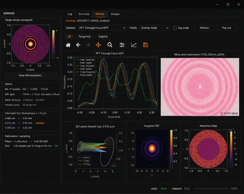
Photonica is the optics and photonics design workflow platform developed by LightBridge. It brings work that normally means moving between several specialist tools into a single workflow you can drive through a visual interface or with Python scripting.

Today it provides a workflow for metalens and metasurface design, covering phase profile handling, geometry mapping from a phase response library, large-scale layout generation and GDS export.

Library generation combines RCWA and FDTD, optical specifications are exchanged through Zemax OpticStudio, and the exported GDS carries straight into prototyping at a foundry.

Photonica Metalens Engine の画面全体。左に設計値パネル、右に MTF、メタアトム配置、3D レイアウト、PSF、波面マップを並べた解析ビュー

TiO₂ / 532 nmSi₃N₄ / 940 nmGDSII


PRODUCTS

Choose the method to match what you are analysing

Nanoscale electromagnetic analysis, circuit-level link analysis, imaging and illumination optics design: each calls for a different method. Tell us the application and we will propose the configuration.

Ansys

Ansys Lumerical

Photonics, electromagnetic, waveguide and multiphysics analysis. Includes FDTD, RCWA, MODE, CHARGE, HEAT, DGTD, FEEM, MQW, STACK, INTERCONNECT and CML Compiler.

FDTDRCWAINTERCONNECT

Ansys

Zemax OpticStudio

Optical design, imaging, physical optics, optimisation and tolerance analysis. Supports sequential and non-sequential ray tracing, stray light analysis and physical optics propagation (POP).

POPTolerancingStray light

Ansys

Ansys Speos

Illumination, optical systems, human vision, stray light and optical performance evaluation. Handles light distribution analysis, visibility evaluation and sensor simulation, for AR / VR, lighting, imaging systems and optical sensors.

Light distributionVisibilitySensors

LightBridge

Photonica

The LightBridge workflow platform for optics and photonics design. It links simulation results to geometry mapping, layout generation and GDS export.

MetalensGDSPython


SOLUTIONS

Find it by application

PHOTONICS

OPTICAL SYSTEMS


FROM DESIGN TO PROTOTYPE

Come in at any stage

There is no need to commission the whole process. Analysis only, or tape-out preparation only, is equally welcome. Start from whichever entry point is closest to where you are now.


WHERE WE ARE USED

Semiconductors, communications, automotive, medical, and research institutes

Semiconductors and photonic devicesCommunications and datacomAutomotive and electronicsSensors and medicalUniversities and national research institutesStartups

Our users include optical engineers, photonics engineers, PIC designers, device physics researchers, analysis engineers, development managers, equipment administrators, technical buyers, founders and CTOs. The analysis methods and product configurations each field needs differ considerably.

Japanese-language support and training

The real work begins after deployment

From licence configuration, installation and system requirement checks through to advice on analysis setup, our technical support team handles it. Past enquiries and their answers are collected in the customer knowledge base.

  • Checking licence configuration and system requirements
  • One-to-one advice on analysis setup, convergence and boundary conditions
  • Hands-on training for each solver
  • Briefings on what changes in every release

TECHNICAL RESOURCES

Analysis notes you can use in practice


Start by telling us the problem you need to solve

It does not matter if you have not chosen a product yet. Tell us the device and what you want to evaluate, and we will tell you which analysis method suits it and how far analysis can take you.

What helps us before we talk

  • Target wavelength and materials
  • Device structure and approximate dimensions
  • The characteristics you want to evaluate, and target values
  • Whether you have existing simulation data or measurements
  • The schedule you have in mind

It is fine if you cannot share all of it. Whatever you are comfortable with is enough.