ANSYS LUMERICAL

Lumerical MODE: waveguide modes and planar circuit propagation

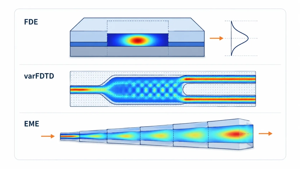
Three solvers: FDE, varFDTD and EME. From mode analysis of a waveguide cross-section to propagation analysis of planar integrated photonic circuits and long tapers, it efficiently handles the problems where 3D FDTD becomes expensive.
FDEvarFDTDEME

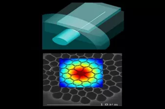
Lumerical MODE analysis example, showing a waveguide structure and the mode profile of a photonic crystal cavity

Overview

From mode analysis to long-distance propagation in one environment

FDE (finite-difference eigenmode) solves the waveguide cross-section as a two-dimensional eigenvalue problem, giving effective index, mode profile, dispersion and propagation loss. Because no propagation calculation is needed, it is extremely fast.

varFDTD reduces a 3D structure to a 2D effective index distribution and analyzes the in-plane behavior with 2D FDTD. It suits planar structures where coupling between different vertical slab modes is weak, and handles propagation in every in-plane direction without assuming an optical axis.

EME (eigenmode expansion) divides the structure into sections of uniform cross-section and connects the modes of each. It handles bidirectional propagation. Once the mode decomposition is done, the propagation length can be changed without redoing the mode calculation, which makes length sweeps and optimization efficient.

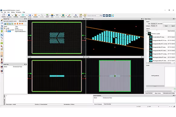
The Lumerical MODE analysis screen, showing the layout of a waveguide structure with several views covering cross-sectional modes through to propagation in the same environment

How MODE’s solvers are arranged

Three solvers to choose from, according to what you are analyzing

01

FDE

Evaluates the eigenmodes of a waveguide cross-section, with effective index, loss and dispersion.

02

varFDTD

Efficient 2.5D analysis of in-plane propagation in planar integrated photonic circuits.

03

EME

Sweeps propagation length efficiently without redoing the mode calculation.

The three Lumerical MODE solvers side by side: FDE showing the eigenmodes of a waveguide cross-section and their profiles, varFDTD showing in-plane propagation in a planar integrated photonic circuit, and EME showing long-distance propagation along a taper

Where it fits

Where it fits, and where it does not

For some problems another method solves faster and more accurately. The following is a guide to choosing.

For structures where coupling between different vertical slab modes is strong, or where out-of-plane radiation and propagation matter, the effective index approximation in varFDTD may not be appropriate. In that case consider EME or 3D FDTD, depending on the problem.

Use MODE when you want to

  • find the effective index and mode profile of a waveguide
  • propagate through a planar circuit of hundreds of µm or more
  • optimize the length of a taper or splitter
  • evaluate bend loss or mode conversion
  • obtain coupling efficiency to a fiber

Consider another method

  • Arbitrary geometry with strong 3D scattering or radiation → FDTD
  • Complex cross-sections with curved or slanted interfaces → FEEM
  • Diffraction efficiency of a periodic structure → RCWA
  • Link performance of the whole circuit → INTERCONNECT

Choose between MODE’s three solvers and the solvers in other products according to the problem and its scale.

Typical applications

Where it is used

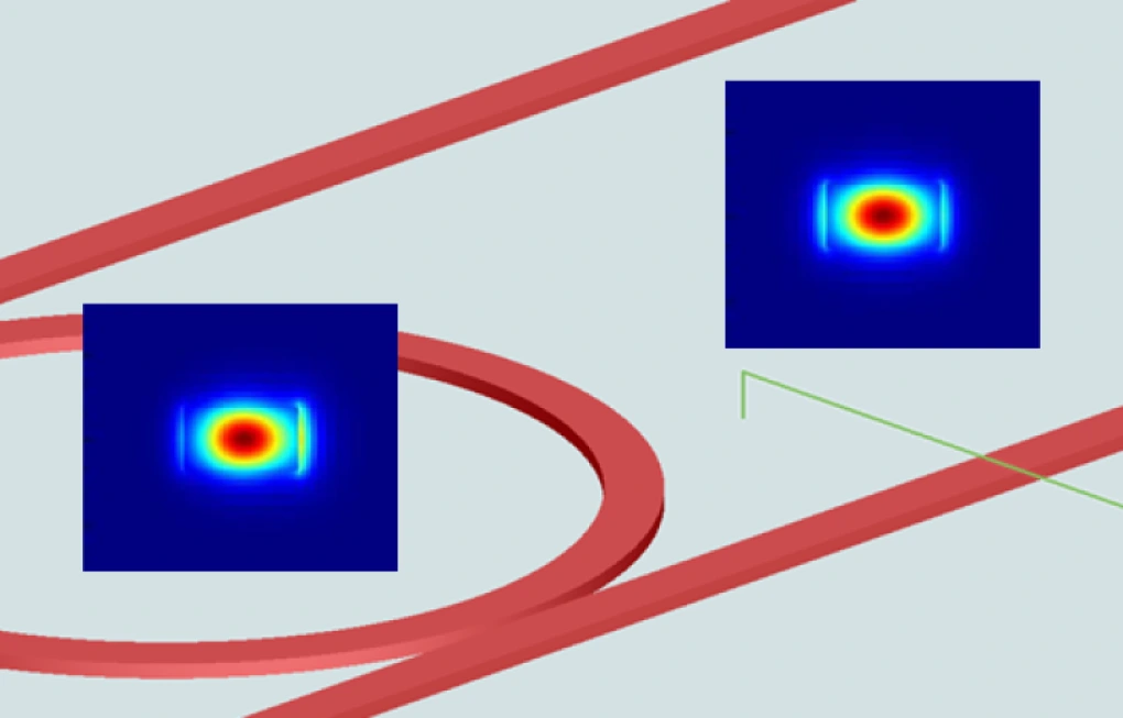
Waveguide analysis with the FDE solver in Lumerical MODE, showing the waveguide layout and two mode field distributions computed on the cross-section

Silicon Photonics

Design of waveguides, directional couplers, MMIs and splitters

View solutions

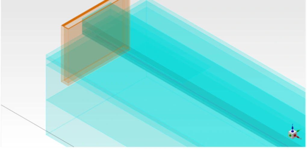
3D model of a fiber-to-chip edge coupler, showing the tapered waveguide and the placement of the EME analysis region

Optical transceivers

Mode design and loss evaluation of modulator waveguides

View solutions

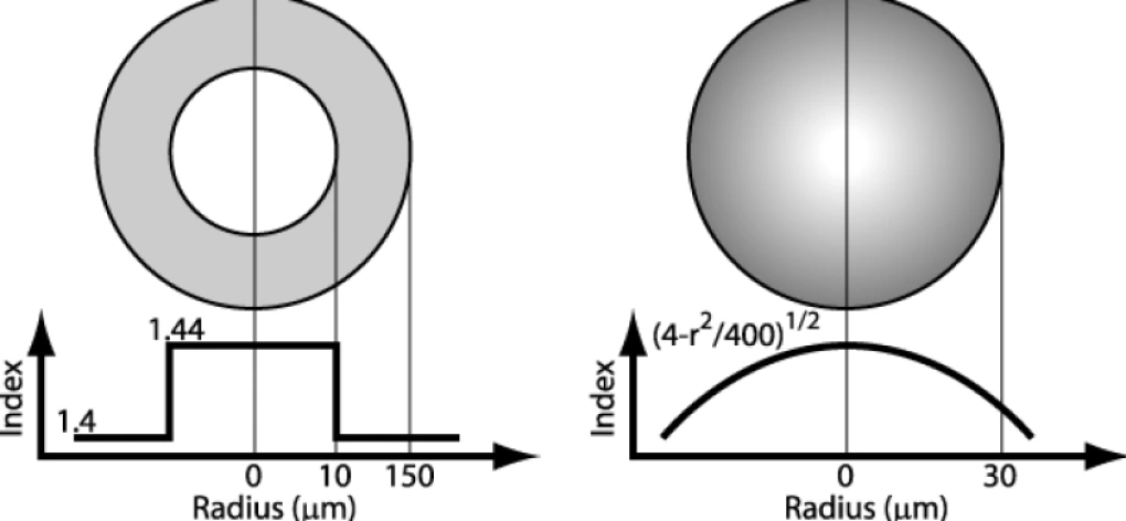
Cross-sections of step-index and graded-index fiber with their radial refractive index profiles

Fiber coupling

Edge couplers and spot size converters

Antenna waveguide layout of an optical phased array, showing the waveguide array and grating with the mode source and monitors in place

LiDAR

Waveguides and splitters in optical phased arrays

View solutions

Inputs and outputs

What you provide, and what you get

Set the cross-sectional geometry, materials, wavelength and device structure, and evaluate mode characteristics, propagation characteristics, S-parameters and more.

INPUT

What you need to prepare

Cross-sectional structureLayer stack, width, thickness, materials
WavelengthA single wavelength, or a sweep range
Number of modesHow many eigenmodes to compute
Propagating structureThe in-plane layout for varFDTD, or the change in structure along the propagation direction for EME

MODE

Waveguide analysis

OUTPUT

What you get

Effective indexn_eff and group index for each mode
Mode profileField profile on the cross-section
S-parametersTransmission and reflection between ports
LossPropagation loss, bend loss, coupling efficiency

Analysis workflow

How it works in practice

In MODE, what matters is choosing the solver that suits the problem and correctly setting up and confirming the mode or propagation characteristic you are after.

01

Define the cross-sectional geometry and materials

Build the cross-section of the waveguide or fiber and assign materials.

02

Choose the solver for the job

Use FDE for cross-sectional modes, EME for long propagation such as tapers, and varFDTD for planar propagation in in-plane devices.

03

Set the analysis region, mesh and boundary conditions

Take a region large enough to contain the evanescent components, then set the number of mesh cells or the maximum mesh step.

04

Set the solver-specific conditions and run

In FDE, set Search near n / in range and Number of trial modes appropriately, and confirm from the mode profiles that the mode you want is in the Mode List. For a wavelength sweep, select the mode of interest and use Track selected mode to follow the same mode.

05

Check the results and carry them into the next design stage

In FDE, check effective index, loss, mode profile and dispersion; in varFDTD, field distribution, transmission, mode coupling and S-parameters; in EME, transmission and reflection between ports and the S-matrix. Where useful, FDE waveguide characteristics or varFDTD and EME S-parameters can be used in a later stage such as INTERCONNECT.

Frequently asked questions

Questions we are often asked about MODE

Questions we are often asked before adoption.

There is no single figure for agreement. varFDTD reduces a 3D structure to a 2D effective index distribution, so it is particularly effective for planar structures where coupling between different vertical slab modes is weak. Under those conditions it can agree well with 3D FDTD. Where coupling between slab modes is not negligible, or where out-of-plane propagation and radiation matter, the varFDTD approximation may not be appropriate, so verify with 3D FDTD where needed.

It suits structures with long propagation distances, such as long tapers, spot size converters, MMIs and periodic devices. Once the mode decomposition is done, the propagation length can be changed without redoing the mode calculation, which makes length sweeps and optimization efficient.

BPM in general uses the slowly varying envelope approximation and presumes a dominant propagation direction. varFDTD assumes no optical axis in-plane and handles propagation in every direction, while EME analyzes propagation including reflection through a bidirectional eigenmode expansion. Which of these solvers to use depends on the problem, for instance high index contrast or long waveguide structures.

Yes. Beam data from Zemax OpticStudio can be brought into MODE via the ZBF format. In FDE you can evaluate the overlap with a mode and the power coupling, and in EME the ZBF data can be imported directly into a Port. MODE results can also be returned to OpticStudio as ZBF.

Japanese-language support and training

We can advise on everything from simulation setup to judging whether a result is sound. Hands-on training is also available.

Helpful to know before we talk

  • Target wavelengths and materials
  • Device structure and approximate dimensions
  • The characteristics you want to evaluate, and your target values
  • Whether you already have simulation data or measurements
  • Your expected schedule

You do not need to share everything. Whatever you are able to tell us is enough.

Try it on the structure you actually need to solve

The demo uses a structure close to your own. We can also give you an idea of the computational scale and the time it takes.