Home/Analysis Technologies/Semiconductor and electrical analysis/CHARGE

Analysis Technologies | Semiconductor and Electrical Analysis

CHARGE (Drift-Diffusion Analysis)

A method that solves Poisson’s equation together with the electron and hole continuity equations to obtain the carrier distribution and current inside a semiconductor device.

Target

Carrier transport in semiconductor devices

Analysis type

Steady state, transient, small-signal AC

Supporting products

Lumerical Multiphysics

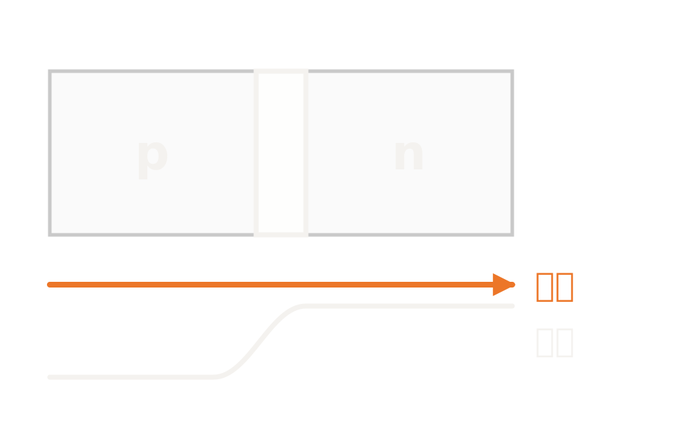
Schematic of a pn junction cross-section showing carrier density and potential distributions and the direction of current

What the method is

Solving carrier distribution and current together

Poisson’s equation for the electrostatic potential, the continuity equations for electrons and holes, and the current density expressions made up of drift and diffusion are solved as a coupled set. Given the doping profile, material models, electrode potentials and, where needed, an optical generation rate, you obtain the carrier concentration distribution, potential, electric field and current.

There are three analysis types. Steady state gives the operating point, transient the time response, and small-signal AC the linear response around the operating point. From the same structural description you can cover DC characteristics, switching and bandwidth under consistent conditions.

Temperature can be handled in three ways: held constant, imported as a temperature distribution obtained elsewhere, or solved self-consistently together with heat conduction. For devices where self-heating affects operation, choose the third.

How it works

Solving Poisson’s equation and the electron and hole continuity equations self-consistently

The drift-diffusion model is a semi-classical description that treats the semiconductor as a continuum. It combines Poisson’s equation for the electrostatic potential, the continuity equations for electrons and holes, and current density expressions writing the electron and hole flows as the sum of a drift term and a diffusion term. Because the three depend on one another, a solution satisfying all of them at once, a self-consistent solution, is found by iteration. Recombination and generation rates enter through the continuity equations.

The formulation was developed to handle numerically the regime where device scaling had made closed-form analytic models untenable. In procedure it is layered: discretize the governing equations, solve the resulting system of nonlinear algebraic equations by iteration, and solve a sparse linear problem inside that.

On the implementation side, the device is divided into an unstructured finite-element mesh and the solution is obtained at each mesh node. The published material does not state which discretization scheme is used for the continuity equations, so this page does not go into the discretization itself.

Governing equationsPoisson’s equation for the electrostatic potential, the electron and hole continuity equations, and the drift-diffusion current density expressions are solved together. Recombination and generation rates enter the continuity equations, and trap-assisted, Auger and radiative recombination can be selected according to the problem.
DiscretizationThe device is divided into an unstructured finite-element mesh and the solution obtained at each mesh node. Mesh density affects both accuracy and convergence.
Nonlinear iterationYou can choose between solving charge and electrostatic potential in separate stages and solving them simultaneously as a coupled set. The latter is more generally applicable but needs a good initial guess.
Boundary conditionsElectrodes are given as conditions fixing the potential. Outer surfaces with no contact take a condition of zero normal electric field. For Schottky contacts, thermionic emission over the barrier and barrier lowering by the field are taken into account.

Strengths of this method

Why this method is chosen

Reaching the regime analytic expressions cannot

For scaled-down devices, closed-form analytic models do not hold. Solving the continuum transport equations numerically is the approach developed to handle that regime.

Three analysis types from one description

Steady state, transient and small-signal AC can all be solved from the same structural description, so operating point, switching and bandwidth can be compared on the same basis.

Physical models you select and combine

Trap-assisted recombination, Auger recombination, radiative recombination, stimulated emission, impact ionization and band-to-band tunneling can be enabled according to the problem.

Where it fits

Where it fits, and where it does not

Where it is a good fit

→ when you need the depletion width and carrier distribution of a pn junction

→ when you need to evaluate the electrical characteristics of an electro-optic modulator

→ when you need dark current, responsivity and 3 dB bandwidth of a photodetector

→ when you want to estimate carrier collection efficiency and quantum efficiency in an image sensor

→ when you want to evaluate the responsivity and conversion efficiency of a solar cell

Where another method is the better fit

Optical response alone: if you want propagation or absorption of light itself, that is the territory of electromagnetic or mode analysis. Carrier transport analysis does not compute optical quantities.

Quantum well gain: the band structure and optical gain of an active layer where quantum confinement matters are handled by a method aimed at quantum wells.

Temperature distribution alone: if the heat generation is known and you only want the temperature distribution, heat conduction analysis on its own is enough.

A whole circuit or link: the performance of a circuit or link built from components is the territory of circuit-level analysis.

Applications

Typical applications

Optical modulators

For a depletion-type phase shifter, obtain the change in carrier distribution against applied voltage.

Photodetectors

Obtain dark current, responsivity and 3 dB bandwidth. The absorption distribution comes from electromagnetic analysis.

Optical transceivers and CPO

Carry the electrical characteristics of modulators and photodetectors into the design of the transmit and receive path.

Solar cells and image sensors

Evaluate conversion efficiency and quantum efficiency from carrier collection efficiency.

Inputs and outputs

What you provide, and what you get

INPUT

Structure Device geometry, with materials assigned per region
Doping The impurity concentration profile per region
Material models Mobility, carrier lifetime, bandgap, effective mass, saturation velocity, recombination coefficients
Excitation Electrode potential or sweep, optical generation rate, imported temperature or heat generation

OUTPUT

Carrier distribution Electron and hole concentration, potential and electric field distributions
Electrical characteristics Current, I-V characteristics, small-signal AC response
Band diagram Band edge distributions from the band structure monitor
Handover data Data files passing carrier distribution or heat generation to optical or heat conduction analysis

How it works

How it works in practice

01

Define the materials and their properties

Take the electrical and thermal properties of semiconductors and metals from the material database. Mobility, bandgap narrowing and recombination models are selected here too.

02

Build the geometry and assign doping

Give the impurity concentration profile per region. For optically driven devices, import the optical generation rate obtained from electromagnetic analysis.

03

Set the analysis type and mesh

Choose between steady state, transient and small-signal AC, and decide how temperature is handled. Place mesh constraints where current density or electric field changes rapidly.

04

Apply boundary conditions, run, and confirm convergence

Settle the electrode potentials and sweep steps and place the monitors. If it does not converge, revisit the step size, the mesh and the physical models you enabled.

The mesh at the junction and how the voltage is stepped decide whether it converges at all. Enabling high-field mobility models or impact ionization makes convergence harder. Step 03 is where most of your time should go.

Relationship to related methods

Division of roles and coupling with related analysis methods

Method Relationship Main targets When to use which
CHARGE (this method) This method Carrier transport in semiconductors Solves Poisson’s equation and the continuity equations self-consistently to obtain carrier distribution and current.
HEAT Coupling Temperature distribution within a structure Can be coupled self-consistently with heat conduction. Electro-thermal analysis including self-heating is that combination.
FDTD Upstream Optical absorption distribution The optical generation rate obtained from absorption is received here as an input. The handover is one-way.
MQW Downstream Quantum well band structure and gain An active layer where quantum confinement matters is handled by a separate method. Carrier density and electric field are passed in a data file and the two are run in sequence.
FEEM Downstream Waveguide cross-sectional modes Receives the index change converted from the carrier distribution as a material and obtains the change in effective index.

View all analysis technologies →

Supporting products

Products that provide this method

A commercial software environment providing electrical analysis based on drift-diffusion. Heat conduction and quantum well analysis sit in the same environment, and handover of data to optical analysis happens there too. See here for licensing, system requirements and deployment.

Lumerical Multiphysics

View the product page →

FAQ

Frequently asked questions

How is data handed over to optical analysis?The carrier distribution obtained is written from a monitor as a data file and read into the optical analysis as an index perturbation. For the conversion there are models based on the plasma effect, and for silicon an empirical expression from the literature. The handover is one-way: optical results do not return to the electrical analysis.
What does small-signal AC analysis give?The linear response around the operating point, in the frequency domain. The 3 dB bandwidth of a photodetector comes from this analysis.
Can it run non-isothermal analysis?Yes. You can import a temperature distribution obtained elsewhere, or solve self-consistently together with heat conduction. The latter is used for devices where self-heating affects operation.
What do I revisit when it does not converge?The voltage step, the mesh, and the physical models you have enabled. High-field mobility models and impact ionization are known to make convergence harder. The iteration method also suits forward and reverse bias differently.

References

Last updated

2026-08-18

Technical review

LightBridge Technical Support

Sources consulted

Ansys Optics: CHARGE solver introductionAnsys Optics: CHARGE solver – Simulation objectAnsys Optics: CHARGE Product Reference ManualAnsys Optics: Semiconductor Material Model PropertiesAnsys Optics: Charge distribution to change in refractive index theoryAnsys Optics: Troubleshooting convergence errors in CHARGE

We can advise on electrical and carrier analysis of semiconductor devices

Tell us the device structure and the characteristics you want to evaluate, and we will propose the method and product that suit.