Home/Analysis Technologies/Semiconductor and Electrical Analysis/MQW

Analysis Technologies | Semiconductor and Electrical Analysis

MQW (Multiple Quantum Well Analysis)

A method that solves the subband structure of a multiple quantum well using the k·p method, and from it calculates optical gain, spontaneous emission and the change in refractive index.

Applies to

The layer structure of a multiple quantum well

Method

Band structure calculation by the k·p method

Available in

Lumerical Multiphysics

Schematic showing the band diagram of a quantum well, the confined wavefunctions, and the path from optical transitions to a gain spectrum

What the method is

From layer structure to gain

Well width, barrier composition, strain. These set the confinement levels and govern the peak wavelength and the magnitude of the gain spectrum. To examine a layer structure before committing to a prototype, you need to be able to follow that relationship by calculation.

The subject is a one-dimensional layer structure along the growth direction. Given carrier density, temperature and bias field as operating conditions, you obtain the subbands and wavefunctions, the gain and spontaneous emission coefficients, and the change in complex refractive index. Gain and spontaneous emission are returned separately for TE and TM.

The assumptions are narrow. What is solved is a one-dimensional layer structure along the growth direction; the stack is treated as extending infinitely in the lateral direction, and the in-plane response is assumed isotropic. Mesa width, lateral confinement and carrier transport across the device sit outside this method and are taken from other methods. It is not a general-purpose method for solving semiconductor devices in three dimensions.

How it works

From electronic states and optical transitions to gain and spontaneous emission

The k·p method describes the motion of electrons and holes in a periodic potential through effective-mass-like equations around the band edge. Where degenerate bands are involved, the description becomes a coupled set of differential equations rather than a single equation. The 4×4, 6×6 and 8×8 options correspond to how many bands are included in that coupled set.

In a quantum well, these equations are solved under the confinement potential along the growth direction to obtain the subband levels and envelope functions — that is, the electron and hole states. The growth direction is discretised by finite differences and the in-plane response is assumed isotropic. Strain enters the Hamiltonian through the deformation potential and shifts the band edges and the effective masses.

Gain is then derived from the optical transitions between the electronic states obtained in this way. Using the transition matrix elements between conduction-band and valence-band states, together with the occupation probabilities under the quasi-Fermi levels set by the carrier density, the stimulated and spontaneous emission coefficients are calculated separately for TE and TM. Intraband scattering is applied as a Lorentzian broadening. The change in refractive index follows from the resulting spectra through the Kramers–Kronig relations.

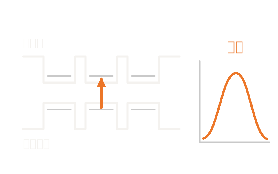
Coupled bandsBecause degenerate bands are involved, a coupled set of equations is solved. The range of bands included corresponds to the 4×4, 6×6 and 8×8 options.
Confinement and envelope functionsThe layer structure along the growth direction is discretised to obtain the subband levels and envelope functions. The solution space is one-dimensional along the growth direction, with the in-plane response assumed isotropic and the structure assumed infinite in the lateral direction.
Handling of strainStrain arising from lattice mismatch enters the Hamiltonian through the deformation potential and shifts the band edges and the effective masses.
Gain and refractive indexThe stimulated and spontaneous emission coefficients are obtained from the transition matrix elements and the occupation probabilities, and the change in refractive index follows from the Kramers–Kronig relations.

What the method is good at

Why this method is chosen

It returns quantities that presuppose quantum confinement

Subband levels, wavefunctions and optical transition matrix elements can be obtained directly — quantities a continuum transport model does not produce.

Results separated by polarisation and operating condition

Stimulated and spontaneous emission can be obtained separately for TE and TM, as functions of carrier density and temperature. What you get is gain parameterised by operating condition, not a single operating point.

You choose the balance of accuracy and computational cost

You choose the range of bands included in the coupled set. Whether a parabolic approximation for the conduction band is sufficient, or coupling between the conduction and valence bands has to be included, can be decided according to the subject.

Where it fits

Where it fits, and where it does not

Where it fits

→ When you want to examine the layer structure of a quantum well laser

→ When you want to estimate the gain spectrum of a semiconductor optical amplifier

→ When you want to evaluate an electro-absorption modulator based on quantum wells

→ When you want the spontaneous emission rate in the active layer of a micro-LED

→ When you want to check how gain depends on carrier density and on temperature

Where another method is the better fit

Carrier transport across the device: injection efficiency into the wells and current–voltage characteristics belong to drift-diffusion analysis. Carrier density and field are taken from there.

Waveguide modes: mode profile, confinement factor and effective index come from mode analysis. The effective index is an input to this method.

The dynamic behaviour of the laser as a whole: threshold current, L–I characteristics and time response belong to circuit-level analysis.

Material systems other than III-V: the scope is mainly III-V zincblende and wurtzite crystals. Other material systems need a different framework.

Applications

Typical applications

Semiconductor lasers

Used to design the layer structure of InP-based and GaAs-based quantum well lasers.

Semiconductor optical amplifiers

Evaluating the bandwidth and the magnitude of the gain spectrum.

Electro-absorption modulators

Evaluating how absorption changes with applied field in modulators based on quantum wells.

Micro-LEDs

Obtaining the spontaneous emission rate in nitride-based active layers.

Inputs and outputs

What you supply, and what you get back

INPUT

Layer structure Thickness and composition of each layer; the well and barrier repeat
Materials k·p parameters, band gap, effective mass, deformation potential
Operating conditions Carrier density, temperature, and bias potential as a function of position
Analysis settings Effective index, linewidth broadening, frequency range, order of the k·p model

OUTPUT

Band structure Band diagram, subband energies, wavefunctions
Gain and spontaneous emission Stimulated and spontaneous emission coefficients, separated into TE and TM
Complex refractive index The change in refractive index, and the attenuation coefficient
Transition data Optical transition matrix elements, quasi-Fermi levels and occupation probabilities

How it is done

How the work actually proceeds

01

Prepare the materials

Supply the k·p parameters, the band gap and the effective mass. For materials that are not in the database, define the electrical properties and the k·p parameters yourself.

02

Set up the layer stack and apply strain

Define the thickness and composition of each layer. Decide the stack with the assumption of infinite lateral extent in mind.

03

Supply the operating conditions

Set the temperature, carrier density, bias field, effective index and linewidth broadening. Carrier density and field can be imported from the results of a drift-diffusion analysis.

04

Choose the solver settings and run

Choose the frequency range, the range of in-plane wavevector and the order of the k·p model, solve, and extract the gain and spontaneous emission spectra.

Use the result of a mode analysis for the effective index. If this does not match the real structure, the absolute value of the gain will be off. Step 03 is where most of the time should go.

Relationship to related methods

Division of work and coupling with related analysis methods

Method Relationship Main subject How they divide up
MQW (this method) This method Band structure and gain of a quantum well Solves the subbands with the k·p method and obtains gain, spontaneous emission and the change in refractive index from the optical transitions.
CHARGE Upstream Carrier transport across the device Obtains the carrier density and field and passes them on as a data file. The two run in sequence; they are not solved simultaneously.
FEEM Upstream Cross-sectional modes of the waveguide Obtains the mode profile and the confinement factor. The effective index becomes an input to this method.
HEAT Upstream Temperature distribution within the structure Obtains the temperature field. The quantum well analysis takes that temperature as a single scalar value.
Circuit-level analysis Downstream Dynamic behaviour of the laser Takes the gain and spontaneous emission spectra and obtains threshold current and L–I characteristics in the time domain.

View all analysis technologies →

Available in

The product that provides this method

A commercial software environment that provides band structure and gain calculation for multiple quantum wells. Drift-diffusion analysis and heat transfer analysis are included in the same environment. To carry a laser design through to completion, however, it is combined with separate products covering mode analysis and circuit-level analysis. See here for licensing, system requirements and adoption.

Lumerical Multiphysics

View the product page →

FAQ

Frequently asked questions

Which material systems are supported?Mainly III-V zincblende and wurtzite crystals. Materials held in the database come with k·p parameters ready; for those that are not, you define the electrical properties and the k·p parameters yourself.
Can strain be handled?Yes. Strain enters the Hamiltonian through the deformation potential and appears in the gain spectrum as a shift in the band edges and the effective masses.
How are carrier transport results used?The carrier density and field distributions obtained from a drift-diffusion analysis are imported as a data file and used as operating conditions. The two analyses run in sequence; they are not solved simultaneously.
How much of a laser’s behaviour can this tell you?What this method gives you is the gain and spontaneous emission spectra of the material itself. To get as far as threshold current, L–I characteristics and modulation response, you combine the confinement factor from a mode analysis with a circuit-level time-domain model. Those are handled by separate products.

Reference information

Last updated

2026-08-18

Technical review

LightBridge Technical Support

Sources consulted

Ansys Optics: Multi-quantum Well (MQW) Solver IntroductionAnsys Optics: MQW Solver PhysicsAnsys Optics: MQW StandaloneAnsys Optics: mqwgain – Script commandAnsys Optics: Multi-Quantum Well (MQW) Edge Emitting LaserAnsys Optics: Material Database in Lumerical Multiphysics (CHARGE, HEAT, DGTD, FEEM, MQW)

Talk to us about quantum well layer structure design

Tell us your layer stack and the characteristics you want to evaluate, and we will suggest the appropriate method and product.