Designing and Analysing Photonic Crystal Nanocavities (FDTD / varFDTD)
How to reproduce and verify the design and analysis of H1 and H2 photonic crystal nanocavities in Lumerical FDTD and MODE varFDTD, covering resonance spectra, symmetric boundary conditions, mode profiles, mesh settings and Q-factor evaluation.
Published
This article uses the analysis of a photonic crystal (PC) nanocavity to explain a simulation approach built around Ansys Lumerical FDTD. The subject is the structure and experimental results reported by Y. Tang et al.; we reproduce the resonance spectra and mode profiles while setting out the reasoning behind the settings and the points to watch. We also touch on an analysis approach using the varFDTD solver in Lumerical MODE and on when to use it rather than FDTD.
This example is not simply a set of steps for reproducing a result. It collects the practical essentials that matter when handling a high-Q structure such as a photonic crystal cavity: mesh settings, boundary conditions (PML and symmetry boundaries), excitation conditions and monitor settings. The material applies well beyond PC cavities, to the analysis of micro- and nano-scale cavities generally.
The simulation file can be obtained from the Ansys Optics application gallery or the Ansys website. Where it is published and how you get to it can change over time, so follow the current guidance.
Summary of results
FDTD can be used to calculate the resonance spectrum of a cavity formed by removing the central hole (H1), or by removing the central hole and the next ring of holes (H2).
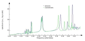
For the H1 cavity, the comparison below uses a constant permittivity model and a physically realistic GaAs/AlGaAs material model. The peak spectra agree well with the published results.
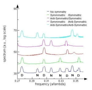
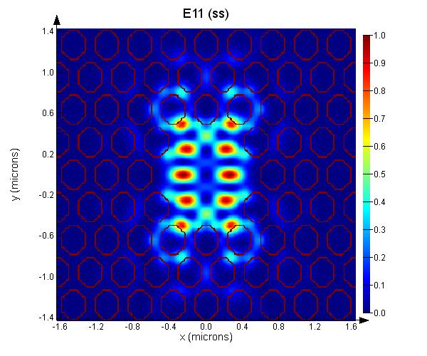
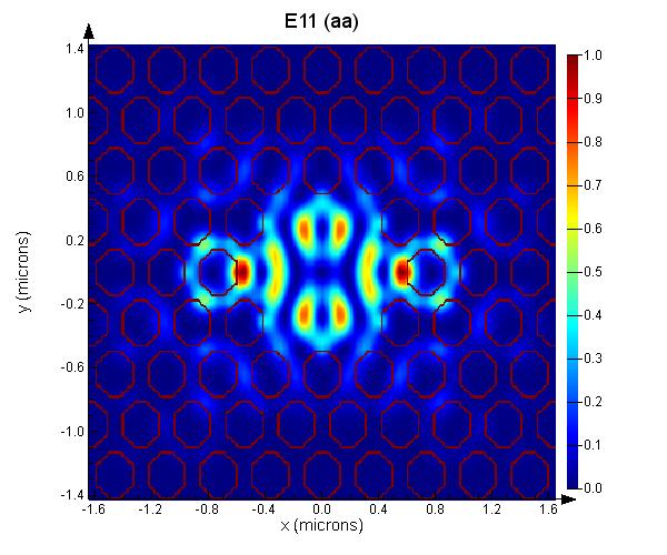
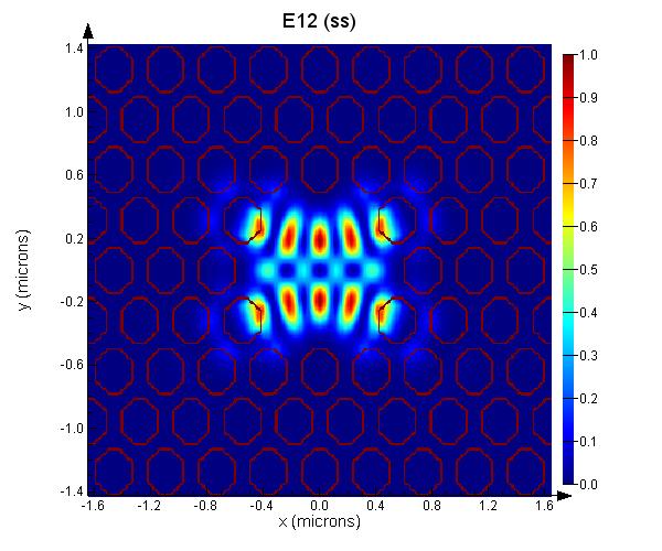
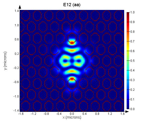
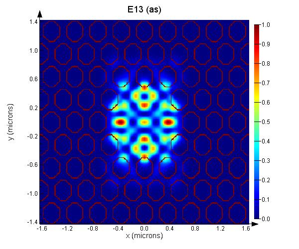
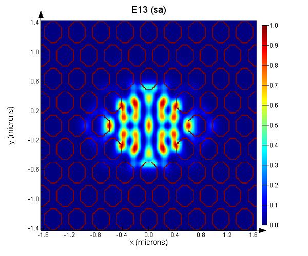
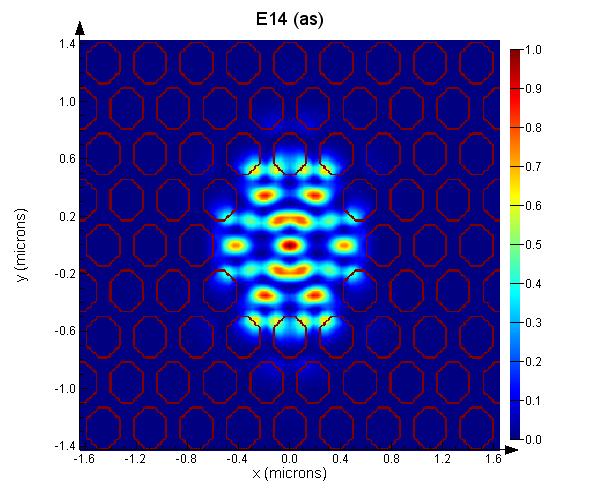
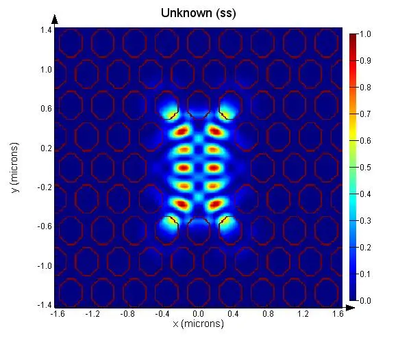
For the H2 cavity we can find the eight resonances reported in the paper in the spectrum. We then separate the degenerate modes using symmetric and antisymmetric boundary conditions.
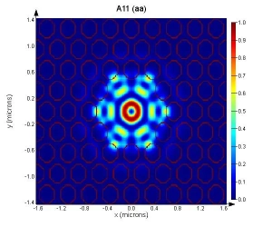
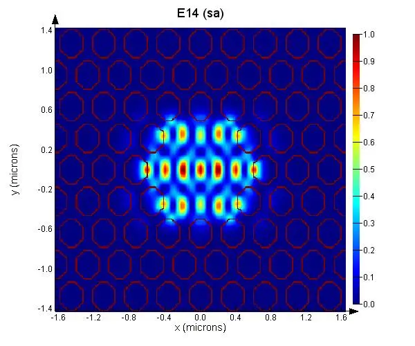
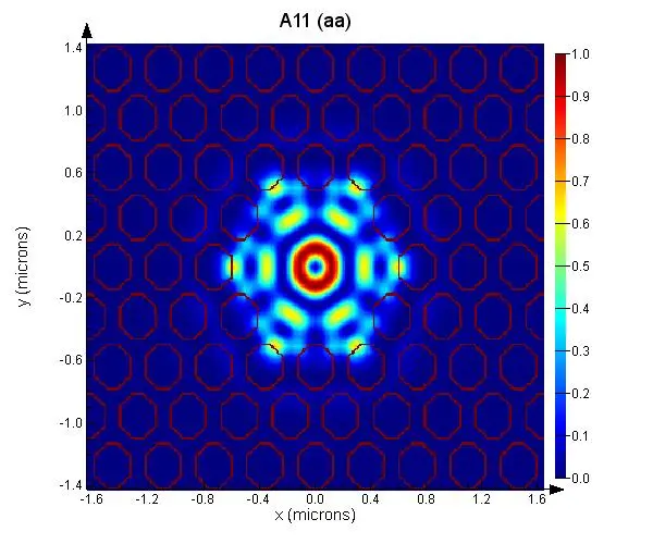
Finally we show how to calculate and plot every mode of the H2 cavity. The A11 mode is shown below as an example.
Simulation setup
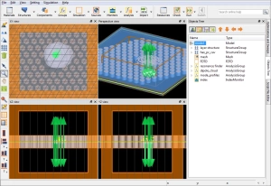
Overview of the structure
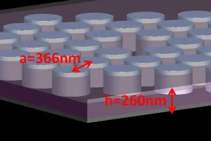
The structure is formed on a thin GaAs/AlGaAs membrane in air. This analysis assumes a layer structure of 170 nm of GaAs sandwiched between 45 nm AlxGa1-xAs layers (x=0.3). Note that in the literature the AlGaAs layers are 40 nm with an additional 5 nm of GaAs on top. That 5 nm layer does not change the results significantly and would require a finer mesh, so we simply use 45 nm rather than 40 nm for the AlGaAs layers. The total layer thickness is 260 nm. This layer structure is contained in a structure group, which allows all layers to use a constant dielectric of n=3.4 (the same value used in the simulations in the literature), Palik experimental data for GaAs, or a theoretical model for AlxGa1-xAs with x=0.3.
The theoretical model was generated by the script AlGaAs_Adachi.lsf, which saves a text file of n and k values that was then imported into the material database as a new material.
The photonic crystal consists of a triangular lattice of holes in the membrane. The lattice pitch a is 366 nm. This example considers a hole radius of 0.37a = 135.4 nm.
The cavity is created using one of the structures in the component library. This structure is fully parameterised, letting you choose parameters such as the pitch and the H number. The hole material is set to etch. The layer structure consists of three rectangles, grouped and parameterised as described above. Finally, the key parameters were added to the model as shown below. These parameters are set by the model and override the direct settings of the child models.
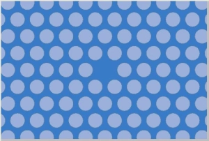
The cavity is created by removing either the central hole (H1) or the central hole and the next ring (H2). This is done by setting the H number of the model to 1 or 2. The H1 cavity is shown below.
Controlling the mesh
For a periodic structure it is best to set the mesh size periodically with respect to the structure. A smaller mesh size means longer compute time and more accurate results. The approach used here is to start with a coarse mesh to obtain initial results and understand the physics of the problem, then move to a finer mesh as needed for the final answer. We control the mesh in x and y by adding a mesh override region and setting the dx and dy values directly. For z, you may choose the automatic non-uniform mesh to select an appropriate mesh. First set the mesh accuracy slider of the simulation region to 2, which controls the z mesh. For the x and y mesh, choose a coarse mesh of 10 points per PC period (a 36.6 nm grid). Because we are using a triangular lattice, set the y mesh cell size to sqrt(3)/2 times the x grid cell size. This gives the FDTD mesh perfect periodicity in the y direction and better accuracy for a given mesh cell size. The model handles this setting, so it is enough to select the “grid points per pitch” property and set it to 10; the model then sets the corresponding dx and dy values.
Simulation region
The second task is to set the size of the simulation region. A larger simulation region takes longer to compute, so we want the smallest region that gives accurate results. For the lateral dimensions of the FDTD region, enough rows of the PC lattice must be included to produce a bandgap. Because this is a PC with high index contrast, three or four rows of holes surrounding the cavity is a good starting point. The x span is 3200 nm and the y span is 3200*sqrt(3)/2, which includes three to four rows of PC holes. Vertically, air must be included above and below the slab because there is an evanescent field decaying into the air. Start by including 500 nm of air above and below the slab. Once you have initial results, run an error analysis to confirm that the simulation dimensions are large enough. This model forces the x and y spans to be integer multiples of the pitch (times sqrt(3)/2 for the y span). If you set the x span to 3200 nm, you may notice on re-editing the object that it has been adjusted to 3294 nm, nine times the 366 nm pitch. Together with the mesh override region settings, this guarantees that the FDTD mesh is identical in every period of the structure, which is important for measuring the Q factor of a periodic device correctly.
Set the simulation time to 2000 fs. Simulation time is discussed in the source properties section.
The boundary condition used when simulating a finite-sized object such as a PC cavity is known as PML (perfectly matched layer). This boundary condition absorbs incident radiation. PML boundary conditions are applied by default when a new simulation region is created. Changing the default PML settings requires two main changes in the advanced options of the FDTD simulation region:
– Uncheck the “extend structure through PML” checkbox. For a photonic crystal, letting the PC extend into the PML improves PML performance. Without this, the last layer of material at the edge of the boundary is automatically extended all the way through the PML.
– Set the “pml kappa” value to 5. PML used together with dispersive materials can lead to increased numerical instability inside the PML. Increasing the PML kappa value keeps the simulation time reasonable.
Where the structure itself is symmetric, symmetry boundary conditions can also be used. They reduce compute time, at the cost of preventing certain modes from appearing in the results (those that do not share the same symmetry as the boundary condition). This PC cavity has a plane of symmetry through the centre of the slab (the z=0 plane). Using a symmetric boundary condition on this plane permits only TE modes and excludes TM modes from the results. Since this structure has little or no TM bandgap and the cavity modes are expected to be TE, we use a symmetric boundary condition here.
Finally, we recommend disabling the FDTD auto shutoff feature when investigating a cavity. The reason is that a high-Q cavity confining light within a very small bandwidth may confine only a small fraction of the original broadband excitation energy. Auto shutoff can then trigger far too early, which can cause problems with time apodisation on the monitors. Auto shutoff can be disabled by unchecking “use early shutoff” on the advanced options tab of the FDTD simulation region.
Pulsed sources and simulation time
Several dipole sources were added to excite the cavity. They are added by an analysis group that creates a random set of dipoles in a given region. That region is controlled by the model and is based on the selected H number (for a larger cavity the dipole group expands). Anticipating simulations with symmetric and antisymmetric boundary conditions, these dipoles are added in the first quadrant only. The sources inject a short pulse of radiation in order to excite a wide range of frequencies. To excite the resonant modes effectively, the polarisation of the dipole sources must be similar to the polarisation of the modes you want to excite. Here we want to excite TE modes, so we use vertically (z) polarised magnetic dipoles. The dipole sources must also be placed where the mode profile does not have a null, which is achieved by setting the dipoles randomly within the region. To excite TM modes instead, you would use vertically polarised electric dipoles and change the zmin boundary condition to antisymmetric. The final step in setting up the source is defining the excitation pulse. This simply means choosing the wavelength range you want to simulate; here we choose 1000 nm to 1400 nm. We used the global source properties so that the settings of each dipole do not have to be changed individually. Note that each dipole must be set to use the global source properties rather than the default settings. The simulation time defined in the simulation region properties is 2000 fs, far longer than the pulse length. This is because we want to monitor the cavity fields after the pulse has excited the modes. Analysing the cavity fields after the initial pulse reveals the frequencies of the cavity modes.
Simulation monitors
The monitors include an analysis group called “resonance finder”. Fourier transforming these time signals reveals the resonant mode frequencies, which the analysis script within the group handles automatically. By default we choose a total of eight time monitors spread randomly through the cavity region. The extent of these monitors is set by the model and depends on the H number chosen for the cavity, which helps avoid the nulls of any particular mode. There are also frequency-domain profile monitors for obtaining the mode profiles. These monitors are held in an analysis group called mode_profiles, which can find the profiles of up to twelve modes. The user must specify the resonant frequency of the mode and the apodisation settings. These settings are extremely important for finding the correct mode profile. For details on apodisation settings, see the User Guide Apodization.
Results: the H1 cavity
The H1 cavity is formed by removing one hole from the photonic crystal, as shown below. This is done by setting the H_number property of the model to 1.
Load Tang_cavity.fsp and run it.
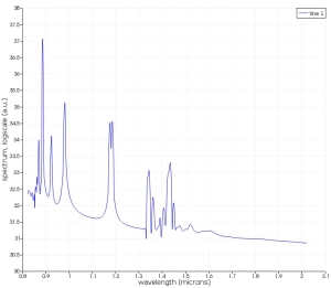
Next, edit the “resonance finder” object and press the “Run Analysis” button to obtain the figures and results below.
The spectrum can also be plotted as a function of normalised units (a/lambda) with the script commands below. The script can be pasted at the script prompt or saved as a new script file.
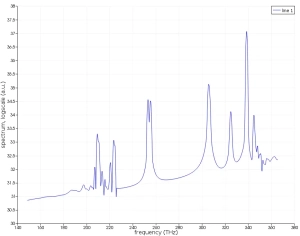
In this example several peaks appear in the results, corresponding to resonant modes and to the bandgap edges. Peaks are often observed at the bandgap edges because modes at those frequencies have very low group velocity and do not decay quickly. The two peaks corresponding to resonant modes appear at about 0.31 and 0.37, in good agreement with the first- and second-order mode results in the Y. Tang paper, which assumed a constant permittivity in the slab waveguide.
Note that the simulation can also be re-run using GaAs and AlGaAs material models, by setting the “use constant dielectric” property of the “layer structure” group to 0. The figure below compares the results.
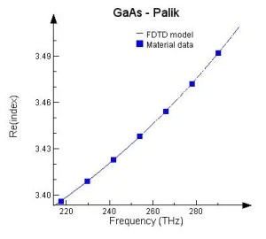
The spectra agree well at low frequency but diverge at high frequency. This shift is consistent with the fact that GaAs occupies 170 nm of the 260 nm layer stack and has a refractive index above 3.4 at high frequency, as shown below.
The rest of this example uses the constant permittivity model. This should agree best with the simulation results of Tang et al., although the dispersive model should agree better with the experimental results.
Next steps
– To determine the mode profiles of the resonant modes, adjust the frequency-domain profile monitor settings (centre frequency and apodisation) and calculate the mode profiles of these resonances. – To learn the symmetry of the modes and see the profiles of degenerate modes, repeat the simulation applying various combinations of symmetric and antisymmetric boundary conditions on the x=0 and y=0 planes. – For more accurate results, repeat the simulation with a finer grid size. It is also worth investigating the effect of moving the PML boundaries further from or closer to the cavity.
The next section demonstrates most of these steps while looking for the H2 resonant modes.
Results: the H2 cavity
To simulate H2, simply change the H_number of the model to 2.
First results
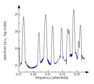
After running the simulation, the script below plots the spectrum in units of normalised frequency (a/lambda).
These results immediately show eight peaks in the frequency range of interest (restricted here to the approximate frequency range where experimental results exist). The peak frequencies are within a few percent of the experimental results, although it is not immediately obvious that each simulated peak matches a particular experimental one. The simulation results contain extra peaks that were not observed in the experimental data. As a first attempt, the agreement is generally very good. Two peaks also appear to be split, which corresponds to a theoretically degenerate peak whose degeneracy has been lifted by the Cartesian mesh. In a triangular lattice, modes can be degenerate on the basis of the 60-degree lattice symmetry. A Cartesian mesh can break that symmetry artificially, and the effect is more pronounced with a coarser mesh. To re-run the simulation with a finer mesh: – Set the “grid points per pitch” property of the model to 20 rather than 10. This halves the dx and dy sizes. – Set the mesh accuracy slider of the FDTD simulation region to 4 rather than 2.
Re-running the simulation (which takes considerable time) lets you compare the fine and coarse mesh results as below. The two agree reasonably, and the frequency shift is generally expected to grow with frequency (that is, at shorter wavelength). You can also see that the finer mesh removes the peak splitting. The coarse mesh is nonetheless surprisingly accurate, particularly considering that lambda0/(n*dx) is about 8 at a wavelength of 1000 nm. This is partly a result of Lumerical’s conformal mesh technology, which makes good results possible at coarser mesh sizes. The rest of this example continues with the coarse mesh. For publication-quality results you would need to repeat the simulation several more times and confirm that the results have converged to within an acceptable tolerance.
Detailed analysis
To understand this problem further, we classify the modes using symmetry and antisymmetry, and calculate the mode profiles using frequency-domain profile monitors. The first step is to add frequency-domain power monitors and configure their frequency and apodisation settings.
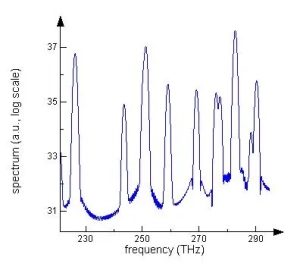
– Apodisation. The simulation runs for 2000 fs. You should choose a time centre of 1000 fs, a time width of 200 fs and full apodisation. This means the FWHM of the apodisation spectrum is 4log(2)/(2pi*200fs) ~ 2 THz. Choosing this apodisation means the correct mode profile can be measured as long as the peaks are more than 2 THz apart and the monitor frequency chosen is within about 2 THz of the correct peak. Plotting the spectrum in unnormalised units shows that this is fine here. For details on apodisation settings, see the User Guide Apodization.
– Frequency settings. We want to add eight monitors with frequencies between 220 and 300 THz. In practice we place nine monitors, to account for the two artificial peaks at 276 THz.
These monitors can be added by hand, but the simulation includes an analysis group called mode_profiles that allows up to twelve frequency monitors to be added in the x-y plane. This makes it easy to adjust the apodisation settings of every monitor at once. To simplify calculating the nine resonant frequencies, the script file Tang_cavity_setup_profile_monitors.lsf calculates the nine resonances within the desired bandwidth and sets the frequencies of the mode_profile analysis group accordingly. The resonant frequencies must be reset whenever the mesh accuracy, material settings or any other setting that could shift the resonant peaks is changed.
Mode symmetry
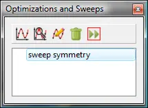
The next step is to consider the symmetry of the modes. We do this by repeating the simulation four times with different combinations of symmetric and antisymmetric boundary conditions on the x=0 and y=0 symmetry planes. Each of these simulations runs in a quarter of the time of the full simulation. This can be done with the “sweep symmetry” object included in this example, found in the “Optimization and Sweeps” window.
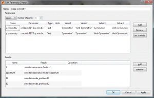
Editing the object shows that it is configured to run four parameter sweeps. Each parameter sweep applies a different symmetry condition to the xmin and ymin boundaries.
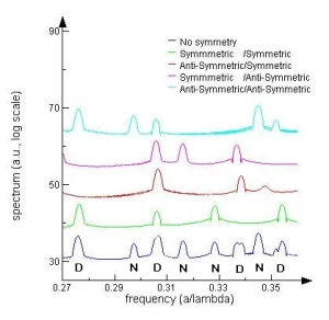
After running the parameter sweep object, the following lines of script plot all the spectra. These lines are also saved in the file Tang_cavity_symmetry.lsf.
The figure below plots the results. The legend indicates whether no symmetry was used, or which symmetry was used on the x-min and y-min boundaries. Symmetric/Anti-Symmetric, for example, means the x-min boundary condition was symmetric and y-min was antisymmetric. In general, some peaks appear for only one combination of symmetry boundaries (non-degenerate modes) while others appear for several combinations (degenerate modes). Each peak in the figure below is marked “D” or “N” to indicate a degenerate or non-degenerate mode.
We can now refer to the experimental results in the Y. Tang paper and identify the simulated modes against the experimental ones. The table below lists the mode frequencies from that paper along with their degeneracy as determined by linewidth and polarisation analysis. This makes it easy to confirm which modes in the simulation data correspond to the experimental data. The results are summarised below.
Peak # (mode)
Degeneracy
Experimental frequency
Simulated frequency
1 (E11) 2 (A11) 3 (E12. E13) 4 (B2)
D N D N
0.285 0.306 0.312 / 0.313 0.323
0.276 0.297 0.307 0.316
5 (A2)
N
0.329
0.328
6 (E14) 7 (A12)
D N
0.341 0.348
0.337/0.339 0.345
8
D
NA
0.354
The results in the table above show that the eighth peak in the simulation data is a degenerate mode slightly above the frequency the quantum dots could excite in the experiment. Knowing that this mode exists, you can see a very small bump around 0.352 in the experimental data that appears to correspond to it.
The simulation data agrees very well with experiment. The worst-case difference between model and experiment is about 3.5%, which matches the worst-case difference of the plane-wave model against experiment. The mean difference in mode frequency between experiment and simulation is under 2%. That is very good agreement for the simple model used here. The result could certainly be improved by using a finer mesh, using a more realistic material model, or confirming that the structural dimensions in the simulation match the device fabricated in the experiment (by using SEM import to define the structure, for example).
Results: mode profiles of the H2 cavity
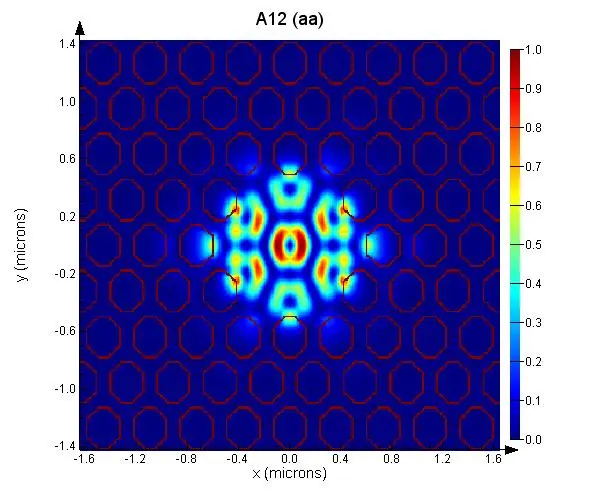
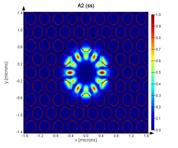
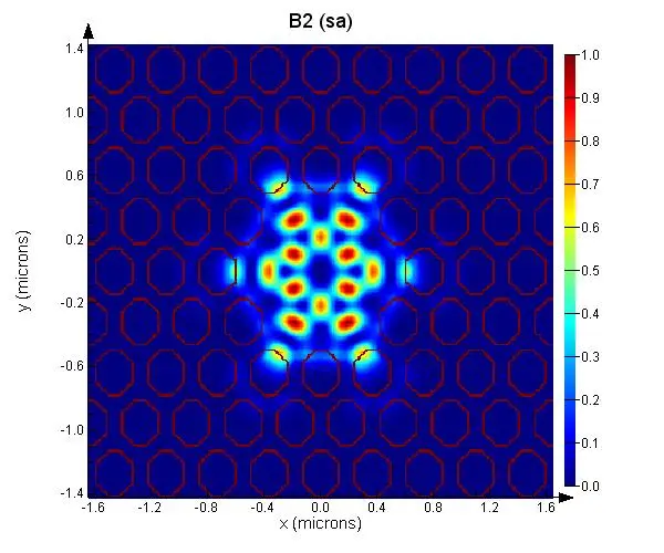
In the previous step we ran several simulations with different symmetries. We also configured the mode_profiles analysis group object with monitors that record the electric field at each of the nine resonant frequencies with appropriate time apodisation. As well as collecting the spectrum for each symmetry setting, the parameter sweep object collects a matrix of |E|^2. This matrix is created by the mode_profiles analysis group during each simulation. The parameter sweep arranges all of this data into a single matrix. At the end of the sweep you have a four-dimensional matrix E2 of size length(x) * length(y) * 9 * 4. The first two dimensions are the x and y axes in the x-y plane. The third dimension corresponds to the nine resonant frequencies collected. The final dimension is the four values of the parameter sweep, corresponding to the four combinations of symmetric and antisymmetric. The script file plot_modes.lsf retrieves the four-dimensional matrix E2. It then interpolates onto a finer mesh, collects an overview of the structure from the index monitors, and builds a higher-resolution matrix so that the results are easier to picture. It then plots various results by selecting a particular resonant frequency and a particular symmetric or antisymmetric condition. Each figure is exported automatically as a jpg file. The results are shown below.
Degenerate modes
Non-degenerate modes
The mode profiles shown here agree very well with the results in the Y. Tang paper, which were calculated using a plane-wave model.
Using the varFDTD solver
The purpose of this section is to show how the varFDTD solver in MODE can be used to analyse the photonic crystal nanocavity below. We do this by reproducing the results of the Y. Tang paper, which contains detailed information on the cavity structure along with experimental and simulation data for comparison.
Setup
The simulation file is cavities_3Dpcm.lms. Overall, setting up a simulation in MODE is very similar to FDTD. The structure can be copied directly from the FDTD sample file, and the simulation region, sources and monitors are configured in the same way. The setup is largely the same, but there are of course a few differences:
– Propagator object, Effective index tab: here we use the default settings, including the Narrowband option, which ignores slab dispersion. Use the Broadband option for greater accuracy.
Results
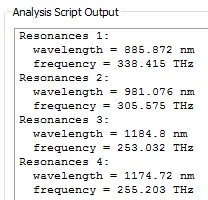
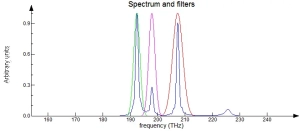
The simulation is very fast and should finish in a few seconds. Next, run the Qanalysis object to find the resonant frequencies. This involves a considerable number of FFTs, so it takes some time. The commands below print the results at the script prompt. The Qanalysis object can be used to plot the spectrum, and the filter used in the calculation.
The amplitude of each resonant peak is not particularly meaningful, since it depends on the position of the source exciting the system and the position of the time monitor measuring the response.
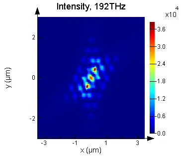
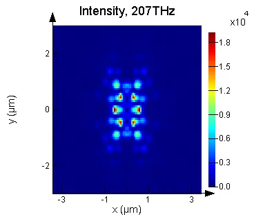
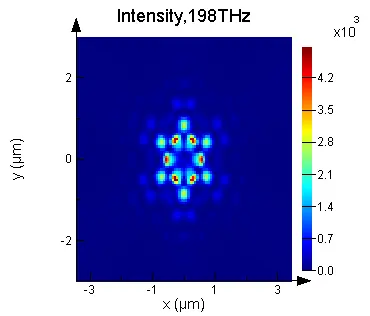
From the calculated resonant frequencies you can set up two profile monitors, one for each frequency, to obtain their profiles.
References
Tang, Y. Mintairov, A.M. Merz, J.L. Tokranov, V. Oktyabrsky, S., Characterization of 2D-photonic crystal nanocavities by polarization-dependent photoluminescence, 5th IEEE Conference on Nanotechnology, July 2005, vol. 1, pp 35-38
We may request cookies to be set on your device. We use cookies to let us know when you visit our websites, how you interact with us, to enrich your user experience, and to customize your relationship with our website.
Click on the different category headings to find out more. You can also change some of your preferences. Note that blocking some types of cookies may impact your experience on our websites and the services we are able to offer.
Essential Website Cookies
These cookies are strictly necessary to provide you with services available through our website and to use some of its features.
Because these cookies are strictly necessary to deliver the website, refusing them will have impact how our site functions. You always can block or delete cookies by changing your browser settings and force blocking all cookies on this website. But this will always prompt you to accept/refuse cookies when revisiting our site.
We fully respect if you want to refuse cookies but to avoid asking you again and again kindly allow us to store a cookie for that. You are free to opt out any time or opt in for other cookies to get a better experience. If you refuse cookies we will remove all set cookies in our domain.
We provide you with a list of stored cookies on your computer in our domain so you can check what we stored. Due to security reasons we are not able to show or modify cookies from other domains. You can check these in your browser security settings.
Google Analytics Cookies
These cookies collect information that is used either in aggregate form to help us understand how our website is being used or how effective our marketing campaigns are, or to help us customize our website and application for you in order to enhance your experience.
If you do not want that we track your visit to our site you can disable tracking in your browser here:
Other external services
We also use different external services like Google Webfonts, Google Maps, and external Video providers. Since these providers may collect personal data like your IP address we allow you to block them here. Please be aware that this might heavily reduce the functionality and appearance of our site. Changes will take effect once you reload the page.
Google Webfont Settings:
Google Map Settings:
Google reCaptcha Settings:
Vimeo and Youtube video embeds:
Other cookies
The following cookies are also needed - You can choose if you want to allow them:
Privacy Policy
You can read about our cookies and privacy settings in detail on our Privacy Policy Page.