
Home/Analysis Technologies/Waveguide and propagation analysis/varFDTD

Analysis Technologies | Waveguide and Propagation Analysis

varFDTD (2.5D Variational FDTD)

A method for planar photonic circuits that uses the vertical slab modes to reduce the structure to effective two-dimensional properties, then solves in-plane propagation with 2D FDTD.

Discretization

In-plane orthogonal grid and time step

Problem solved

2D FDTD on effective 2D properties

Supporting products

Lumerical MODE
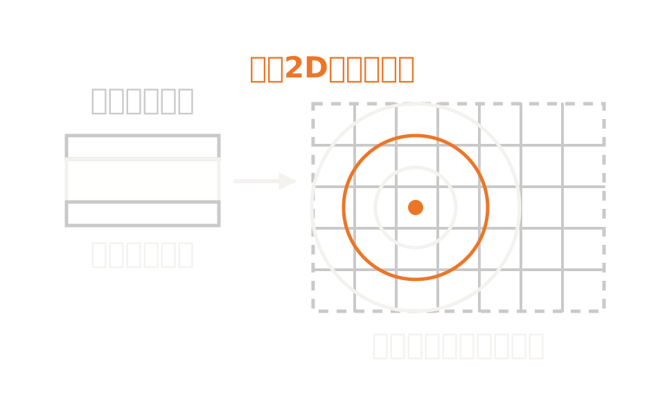
Diagram showing the vertical direction of a layered structure reduced to effective two-dimensional properties, with propagation solved on an in-plane two-dimensional grid

What the method is

Collapse the vertical direction, solve in-plane in the time domain

varFDTD handles light propagation in planar integrated optics, from ridge waveguide systems through to complex geometries such as photonic crystals. What distinguishes it is that it assumes no propagation axis and can propagate in every in-plane direction.

The calculation proceeds in three stages. First the vertical slab modes of the core structure are obtained over the wavelength range of interest. Then the structure is meshed and, taking the slab mode profile into account, the layer stack at each point is replaced by effective two-dimensional properties, collapsing the vertical degree of freedom. Finally that two-dimensional structure is solved with 2D FDTD. The fields can be expanded back into three dimensions if required.

MODE provides several methods for that reduction: one based on a variational formulation and one based on the reciprocity theorem. Both produce dispersive effective materials that include material and waveguide dispersion, and fit them to a material model usable in a time-domain calculation. The method’s name comes from the variational formulation, but the reduction procedure is not limited to it.

How it works

Reduce the vertical direction to effective 2D properties, then step in time with 2D FDTD

At the center of the method is the approximation of fixing the vertical field profile in advance. A reference slab mode profile is fixed, and an integral weighted by that profile replaces the layer stack at each point with a single effective permittivity. The vertical degree of freedom is not solved, it is reduced away. The reduced two-dimensional structure is then solved on the same grid and time step as an ordinary 2D FDTD.

The method’s main assumption is that there is almost no coupling between the several slab modes supported. For a slab structure such as SOI that supports only two modes vertically, this is a very good assumption. Where vertical coupling or radiation matters, on the other hand, the assumption shows up as a systematic difference in the result. It does not produce results equivalent to 3D FDTD.

Identify the slab modesObtain the vertical slab modes of the core structure over the wavelength range of interest. Specify the reference point and the polarization.
Reduce to effective 2D propertiesWeight by the reference slab mode profile and replace the layer stack at each point with effective two-dimensional properties. MODE provides a variational method and a reciprocity-theorem method.
Time stepping with 2D FDTDSolve the reduced two-dimensional structure as 2D FDTD on an orthogonal grid with a time step. No propagation axis is assumed.
Check the effective materialsThe reduction can produce unphysical refractive indices. An option is provided to constrain them to the range of the original materials.

Strengths of this method

Why this method is chosen

In-plane propagation with no propagation axis

Handles propagation in every in-plane direction with no assumption about an optical axis. Structures where light circulates, such as ring resonators and photonic crystal cavities, are within scope.

Large planar layouts

Because three-dimensional geometry is reduced to effective two-dimensional properties, the cost stays at two-dimensional scale. Devices on the scale of hundreds of micrometers can be handled quickly.

Preserves the slab physics

The group index within the slab is handled correctly, and near-to-far-field transformation uses a function appropriate to propagation within a slab. Diffraction of guided modes can be studied without taking a large analysis region.

Where it fits

Where it fits, and where it does not

Where it is a good fit

→ when you want to handle structures where light circulates in-plane, such as ring resonators and photonic crystals

→ when you want to evaluate a planar layout on the scale of hundreds of micrometers in a realistic time

→ when you want a spectrum over a wide wavelength range from a single run

→ when you want to sweep design parameters to see the trend and narrow down the geometry

→ when you want to look at diffraction within the slab, or how light spreads out of a waveguide

Where another method is the better fit

Structures where vertical coupling or radiation matters: because vertical coupling is treated as absent, coupling efficiency comes out too high. Vertical loss is not included either, so spectral peaks come out higher than in a three-dimensional calculation. In a ring resonator comparison, that difference is real and visible.

When final accuracy is required: this method suits the stage of studying the effect of design parameters, and optimization. For verifying results and securing final accuracy, use the slower three-dimensional time-domain calculation or eigenmode expansion.

Structures that are not planar: the method presumes a planar structure extruded in the vertical direction. It does not suit structures whose shape changes substantially in the vertical direction, or where coupling between slab modes cannot be neglected.

Length sweeps of long devices: for sweeping the length of a device whose shape changes gradually along the propagation direction, such as a taper, eigenmode expansion is more efficient because changing the length costs almost nothing extra.

Applications

Typical applications

Ring resonator design

Study free spectral range and resonance trends quickly and narrow down dimensions. Because vertical coupling is not included, confirm the final values with a three-dimensional calculation.

Arrayed waveguide gratings and star couplers

Evaluate the distribution and phase per wavelength, including diffraction in the slab region.

Photonic crystal waveguides

Study the band structure and propagation behavior of a line-defect waveguide.

Evaluating large planar layouts

Evaluate planar circuits at a scale awkward for three-dimensional time-domain calculation, at two-dimensional cost.

Inputs and outputs

What you provide, and what you get

INPUT

Planar structure A planar photonic circuit built from geometry extruded in the vertical direction
Slab mode reference The coordinates of the reference point at which the effective index is obtained, and the polarization of the slab mode
Reduction method The variational method, or the reciprocity-theorem method
Bandwidth handling A setting that uses the center frequency only, and a broadband setting that produces dispersive effective materials
Mesh and boundary conditions Grid density, the time step stability factor, and boundary conditions such as PML
Sources and monitors The wavelength range and incident mode of the mode source, and the placement of the various monitors

OUTPUT

Transmission and reflection Transmission and reflection spectra from frequency-domain power monitors
Field distribution Field distributions and time waveforms from cross-sectional profile monitors and time monitors
Effective index Effective index as a function of frequency, returned by the effective index monitor
Mode expansion results The transmitted component into each mode, from a mode expansion monitor
Far field The result of a near-to-far-field transformation appropriate to propagation within a slab

How it works

How it works in practice

01

Build the planar structure

Build the planar circuit from geometry extruded in the vertical direction and assign materials.

02

Settle the slab mode reference

Place the analysis region, put the reference point at which the effective index is obtained on the core, and choose the slab mode polarization and the effective index method.

03

Set the bandwidth and mesh

Decide whether to use the center frequency only or to produce dispersive effective materials, and set the grid density. Confirm that the effective materials produced fall within a physical range.

04

Run and confirm convergence

Take a run time long enough for the fields to decay sufficiently, then vary the grid and settings and confirm that the result does not move.

Frequency-domain monitor results are not correct if the run is cut short before the fields have decayed sufficiently. Allow a generous run time. A convergence check is needed both for this method and for the three-dimensional time-domain calculation. Once the design is narrowed down, verify with the three-dimensional calculation.

Comparison with related methods

Choosing between related analysis methods

Method Relationship Main targets When to use which
varFDTD (this method) This method Wide planar structures Reduces the vertical direction to effective two-dimensional properties and solves in-plane propagation with 2D FDTD. No propagation axis is assumed.
FDTD Complementary Evaluation including vertical coupling and radiation Discretizes the analysis region as a volume. Because it includes vertical loss, in the comparison example the peaks are lower and the resonant wavelengths differ. Used for final confirmation.
EME Alternative Long devices whose shape changes gradually along the propagation direction Connects scattering matrices on a basis of cross-sectional modes. It is strong for length sweeps, while broadband results come more easily from this method: the two divide the work between them.
FDE Upstream The cross-sectional modes themselves Solves the cross-sectional eigenvalue problem to obtain the modes. Used for deciding the incident mode and for checking the effective index.

View all analysis technologies →

Supporting products

Products that provide this method

A commercial software environment for waveguide and optical coupling analysis. Alongside the 2.5D variational FDTD method, finite-difference eigenmode analysis and eigenmode expansion solvers sit in the same environment, so you can go from cross-sectional modes to propagation across a whole planar circuit without leaving it. See here for licensing, system requirements and deployment.

Lumerical MODE

View the product page →

FAQ

Frequently asked questions

Will it give the same result as a three-dimensional time-domain calculation?No. In the ring resonator comparison the free spectral range agrees and the trend is the same, but the peak height and wavelength shift. Vertical coupling is treated as absent, so coupling efficiency comes out too high, and vertical loss is not included, so peaks come out higher. Use it for design exploration and confirm finally with a three-dimensional calculation.
How much faster is it?It depends on the structure. The only figures we could confirm are from the ring resonator example, where under those conditions memory was less than one fifteenth and run time less than one hundredth. That ratio does not hold generally, so check it for your own case.
What structures does it not suit?Structures whose shape changes substantially in the vertical direction, and structures where coupling between several slab modes cannot be neglected. The method’s main assumption is that there is almost no coupling between the slab modes supported.
Which of the two effective index methods should I choose?MODE has a variational method and a reciprocity-theorem method, and both produce dispersive effective materials that include material and waveguide dispersion. There is no single rule for choosing, so the reliable approach is to compute with both and check the difference.

References

Last updated

2026-08-19

Technical review

LightBridge Technical Support

Sources consulted

Ansys Optics: MODE – 2.5D varFDTD solver introductionAnsys Optics: varFDTD solver – Simulation objectAnsys Optics: My First Simulation – Ring Resonator – Comparison to 3D FDTDAnsys Optics: Ring resonator getting started – Design and initial simulationAnsys Optics: Curved waveguide taper (varFDTD and FDTD)Ansys Optics: Arrayed waveguide grating (AWG)Ansys Optics: Effective index monitor – Simulation objectAnsys Optics: MODE product reference manual

We can advise on propagation analysis of planar photonic circuits

Tell us the scale of the circuit and the characteristics you want to evaluate, and we will propose the method and product that suit.