Coupling Fibre to a Photonic Chip: a Microlens and Edge Coupler Approach
How to design coupling from an optical fibre into a photonic chip using a microlens and an edge coupler: fibre mode analysis in Lumerical MODE, alignment evaluation with POP in OpticStudio, and analysis of the coupling region with FDTD and EME.
Published
Overview
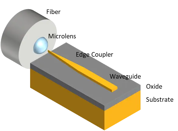
This article sets out in detail how to couple light from an optical fibre into a photonic chip using a microlens and an edge coupler. The approach uses Ansys LumericalandAnsys Zemax OpticStudio, combining FDTD (finite-difference time-domain) and POP (physical optics propagation) so that coupling efficiency and power loss under misalignment can be quantified, supporting an efficient design with low insertion loss.
Why fibre-to-chip coupling matters
In photonics, fibre-to-chip coupling is extremely sensitive: a small offset or alignment error has a large effect on the whole system. A workflow that links Lumerical and OpticStudio is effective for optimising this process, and evaluating coupling performance under a range of conditions reduces development cost while achieving efficient coupling.
The workflow in detail
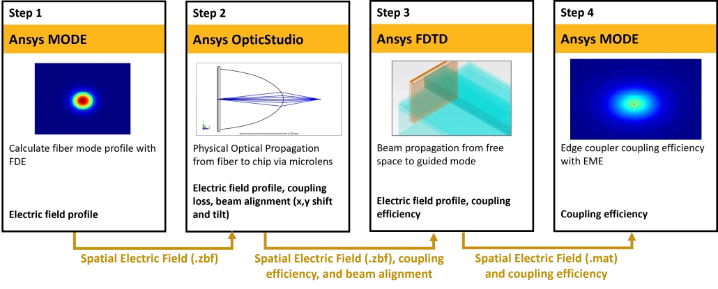
Step 1: fibre mode analysis in Lumerical MODE
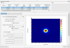
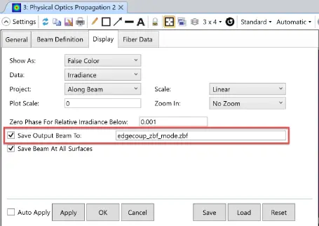
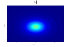
The first step is to use the Lumerical MODE FDE (finite-difference eigenmode) solver to analyse the fibre modes and export the field in ZBF format. This also handles single-mode fibres that are not Gaussian (SMF-28, for example), and lets you set parameters such as core radius and cladding index.
Step 2: aligning the microlens in OpticStudio
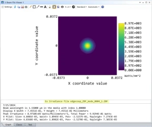
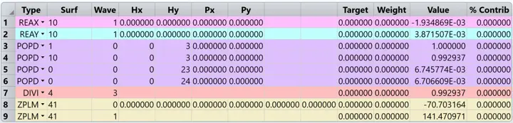
Next, model the microlens using POP analysis in OpticStudio and simulate field propagation from the fibre to the chip facet. Set horizontal and vertical translation and rotational offsets to evaluate coupling performance under complex alignment conditions. The resulting fields and parameters are then exported for use in the next stage of analysis.
Step 3: conversion from free space to a guided mode (Lumerical FDTD)
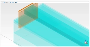
Next, import the field exported from OpticStudio into Lumerical FDTD and set it as a custom source. This allows electromagnetic propagation from free space into the waveguide to be simulated accurately, and lets you verify the loss and coupling performance of the final input field.
Step 4: mode conversion in the spot-size converter with the EME solver
Finally, use the EME solver in Lumerical MODE (eigenmode expansion) to carry out mode conversion in the spot-size converter of the edge coupler and calculate the final coupled power. This method suits SSC device simulation in particular, which is computationally demanding, and evaluates coupling performance efficiently and accurately.
Key settings and optimisation points
POP sampling and data export
Importing and exporting the electric field as ZBF data is central to this workflow. Export from Lumerical requires uniform spatial sampling, and the OpticStudio settings add a guard band on resampling to prevent diffraction artefacts.
Choosing the alignment variables
Accounting for the relative position and rotational offset between the fibre and the microlens improves the robustness of the coupling. Considering tilt misalignment about the X and Y axes as well adds further accuracy.
Improving convergence of the EME solver
Setting an optimised number of modes, transverse mesh resolution and cell count keeps the simulation accurate while remaining computationally efficient. Adjusting the coefficients of the forward-propagating modes improves coupling performance further.
Extending and automating the model
For more advanced analysis or automation, this workflow can be integrated with Ansys optiSLang to handle complex design scenarios. Linking the OpticStudio and Lumerical modules provides a comprehensive design environment covering parametric analysis, alignment tolerance settings and yield analysis.
Practical applications
As photonic chip integration advances, co-packaging optical components in 3D integrated circuits is becoming increasingly important. This workflow is expected to deliver efficient design, cost reduction and improved system reliability, making it an essential tool in modern photonic system design. Using a microlens and an edge coupler optimises coupling performance between fibre and photonic chip, and is expected to form the basis of advanced photonics applications.
We may request cookies to be set on your device. We use cookies to let us know when you visit our websites, how you interact with us, to enrich your user experience, and to customize your relationship with our website.
Click on the different category headings to find out more. You can also change some of your preferences. Note that blocking some types of cookies may impact your experience on our websites and the services we are able to offer.
Essential Website Cookies
These cookies are strictly necessary to provide you with services available through our website and to use some of its features.
Because these cookies are strictly necessary to deliver the website, refusing them will have impact how our site functions. You always can block or delete cookies by changing your browser settings and force blocking all cookies on this website. But this will always prompt you to accept/refuse cookies when revisiting our site.
We fully respect if you want to refuse cookies but to avoid asking you again and again kindly allow us to store a cookie for that. You are free to opt out any time or opt in for other cookies to get a better experience. If you refuse cookies we will remove all set cookies in our domain.
We provide you with a list of stored cookies on your computer in our domain so you can check what we stored. Due to security reasons we are not able to show or modify cookies from other domains. You can check these in your browser security settings.
Google Analytics Cookies
These cookies collect information that is used either in aggregate form to help us understand how our website is being used or how effective our marketing campaigns are, or to help us customize our website and application for you in order to enhance your experience.
If you do not want that we track your visit to our site you can disable tracking in your browser here:
Other external services
We also use different external services like Google Webfonts, Google Maps, and external Video providers. Since these providers may collect personal data like your IP address we allow you to block them here. Please be aware that this might heavily reduce the functionality and appearance of our site. Changes will take effect once you reload the page.
Google Webfont Settings:
Google Map Settings:
Google reCaptcha Settings:
Vimeo and Youtube video embeds:
Other cookies
The following cookies are also needed - You can choose if you want to allow them:
Privacy Policy
You can read about our cookies and privacy settings in detail on our Privacy Policy Page.