
Home/Analysis Technologies/Thin-film analysis/STACK

Analysis Technologies | Thin-Film Analysis

STACK (Multilayer Thin-Film Analysis)

A method for multilayer structures whose layers are flat and laterally uniform. An analytic transfer matrix formulation gives reflection and transmission, the fields within the film, and emission from inside a layer. Because there is no discretization, no convergence check is needed.

Formulation

Analytic transfer matrix

Problem solved

Reflection, transmission and internal fields of a flat multilayer

Supporting products

Lumerical FDTD
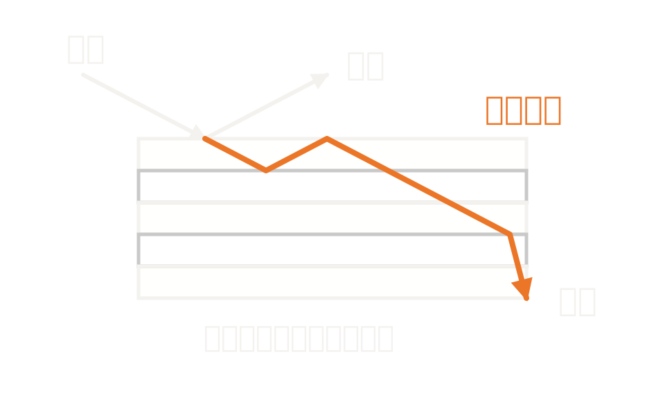
Diagram showing a plane wave incident obliquely on a flat multilayer stack, undergoing multiple internal reflections and dividing into reflection and transmission

What the method is

Treating a stack of flat layers analytically

The optical response of a multilayer structure can often be obtained analytically rather than by simulating Maxwell’s equations directly. STACK is the set of solutions for that purpose. In practice it is a set of script functions, with equivalent graphical objects also provided.

At its center is the ability to obtain plane-wave reflection and transmission from an analytic transfer matrix formulation. The same formulation also gives the distribution of the electric and magnetic fields inside the film. There is a further capability for emitters placed within a layer, giving the angular distribution of the radiation and the Purcell factor within the same framework.

The only inputs required are the refractive index and thickness of each layer and the range of illumination angle and frequency. With no mesh and no time step there is no convergence to confirm. What decides whether the result is valid instead is the judgment of whether the target can be represented as a plane-layered stack at all.

How it works

Replace each layer’s contribution with a matrix, and join them at the boundaries

Each layer is represented by a matrix determined by its complex refractive index and thickness and by the frequency and angle of incidence given. Multiplying the layer matrices in order, between the incident and exit media, gives the complex reflection and transmission coefficients for s- and p-polarization; the power fractions follow from those. Fields within the film are reconstructed by returning the forward and backward components at each interface.

How far multiple-reflection interference is taken into account varies with the target. When studying quantum efficiency or extraction efficiency in a microcavity, handling interference from multiple reflections is essential. Once a layer thickness reaches the order of the coherence length, on the other hand, interference is dropped.

AssumptionsThe premise is that the layers are flat and laterally uniform. In-plane patterns do not enter this formulation.
Layer matricesEach layer is replaced by a matrix determined by its complex refractive index, thickness, the frequency and the angle of incidence.
ConnectionThe matrices are multiplied together between the incident and exit media to give complex reflection and transmission coefficients per polarization.
Handling emissionFor an emitter placed within a layer, there are capabilities to obtain the angular distribution of the radiation, the Purcell factor, and the quantum and extraction efficiencies analytically.

Strengths of this method

Why this method is chosen

No error from discretization

Because the formulation is analytic there is no mesh and no time step. A time-domain calculation approaches this result as the grid is refined; in a comparison, the analytic STACK solution is the reference.

Strong for sweeps

For multilayer structures, obtaining the fields is far more efficient than a time-domain calculation, and the gap widens the more conditions you run. The Purcell factor is obtained for every dipole position in a very short time.

Emitting devices in the same framework

Beyond reflection and transmission, the radiance, luminance and chromaticity of a dipole placed within a layer, and the Purcell factor, are all obtained in the same framework.

Where it fits

Where it fits, and where it does not

Where it is a good fit

→ when you are settling the layer stack of an antireflection coating or a dielectric multilayer mirror

→ when you want to study reflection and transmission densely against angle of incidence and wavelength

→ when you need the field distribution inside the film to know where absorption occurs

→ when you want to move the emitting layer and compare extraction efficiency and Purcell factor

→ when you want to settle the underlying layer stack before designing an in-plane pattern

Where another method is the better fit

Structures with an in-plane pattern: structures whose geometry varies laterally are outside this formulation. If there is a period you need a method that expands in the Fourier domain; if there is none, a time-domain method.

Finite size or arbitrary geometry: structures that cannot be represented as a plane-layered stack are out of scope. The edges of an element and the effect of finite size itself are not included.

Layers thicker than the coherence length: once a layer thickness reaches the order of the coherence length, interference from multiple reflections is dropped. Keeping a thick substrate coherent does not match reality.

The guided modes themselves: once the layer stack is settled, if you want the modes of a waveguide, move to a method that solves the cross-sectional eigenvalue problem.

Applications

Typical applications

Optical thin-film design

Settle the layer stack of an antireflection coating or dielectric multilayer mirror, including its angular and spectral dependence.

Solar cells

Obtain absorption within the absorbing material from the field distribution in the film, and carry that through to an estimate of short-circuit current.

OLEDs and micro-LEDs

Vary the position of the emitting layer and compare far-field power density, quantum efficiency and extraction efficiency.

The layers beneath a metasurface

Settle the substrate and underlying layer stack before designing the in-plane pattern.

Inputs and outputs

What you provide, and what you get

INPUT

Layer stack The thickness and refractive index of each layer, with the incident and exit media at either end
Material Wavelength-dependent complex refractive index. Isotropic and anisotropic materials can both be specified, with or without dispersion
Illumination conditions The set of frequencies and the angle of incidence
Field settings The range and resolution of the positions at which fields are obtained
Emission conditions Dipole position and orientation, emission spectrum, angular resolution

OUTPUT

Reflection and transmission Power fractions per polarization, and complex reflection and transmission coefficients
Fields within the film Electric and magnetic fields as a function of position
Angular distribution of radiation Radiance, luminance and chromaticity as a function of radiation angle
Purcell factor Purcell factor against dipole position, and power density upward and downward

How it works

How it works in practice

01

Lay out the layer stack

List the material and thickness of each layer in order, from the incident medium to the exit medium. What you set here more or less decides the result.

02

Settle the illumination conditions

Set the frequencies and the angle of incidence. Where angular dependence is needed, give the angle as an array too.

03

Choose the quantities you need

Choose from reflection and transmission, fields within the film, dipole emission within a layer, and the Purcell factor, and give the corresponding settings.

04

Evaluate the results

Extract and evaluate reflection and transmission per polarization, the field distribution within the film, the angular distribution of radiation, and the Purcell factor.

No convergence check is needed, but the judgment of whether the target can be represented as a plane-layered stack decides everything. The moment an in-plane pattern appears, the premise of the method breaks. Where thick layers are involved, confirm whether multiple-reflection interference should still be taken into account.

Comparison with related methods

Choosing between related analysis methods

Method Relationship Main targets When to use which
STACK (this method) This method Flat, laterally uniform multilayer structures Multiplies layer matrices together to obtain reflection and transmission, the fields within the film and emission from within a layer analytically. There is no discretization, and no convergence check is needed.
RCWA Alternative Layered structures with in-plane periodicity Expands in-plane in the Fourier domain and solves layer by layer to give the response per order. The moment a lateral pattern appears, you move to this.
FDTD Alternative Arbitrary geometry or finite size Discretizes the analysis region as a volume. Use it for structures that cannot be represented as a plane-layered stack, or when the effect of an element’s edges has to be included.
FDE Downstream Guided modes once the layer stack is settled Solves the cross-sectional eigenvalue problem to obtain the modes. Used at the stage after the vertical layer stack is settled.

View all analysis technologies →

Supporting products

Products that provide this method

A commercial software environment for optical analysis of thin films and fine structures. Alongside the analytic multilayer solution, a three-dimensional time-domain solver and rigorous coupled-wave analysis sit in the same environment, so you can go from flat layers to in-plane patterns without leaving it. See here for licensing, system requirements and deployment.

Lumerical FDTD

View the product page →

FAQ

Frequently asked questions

Is no convergence check really needed?None, because there is no discretization. What decides the result instead is the judgment of whether the target can be represented as a plane-layered stack. Where thick layers are involved, also confirm whether multiple-reflection interference should still be taken into account.
Can it give absorption within a layer?The distribution of the electric and magnetic fields within the film is available, so absorption is evaluated from the field intensity inside the absorbing material. In solar cell design this distribution is carried through to short-circuit current. As far as we could confirm, there is no output that returns absorption per layer directly.
Can it be used to evaluate emitting devices?Yes. There is a capability to place a dipole within a layer and obtain radiance, luminance, chromaticity and the Purcell factor. In practice you first look at the field distribution within the film to find where the field is strong, then place a dipole there and vary its position.
Can it handle anisotropic materials?Yes. Refractive index can be given for isotropic and anisotropic materials alike, with or without dispersion. Fully anisotropic dispersive materials are supported.

References

Last updated

2026-08-19

Technical review

LightBridge Technical Support

Sources consulted

Ansys Optics: STACK Optical Solver OverviewAnsys Optics: STACK Product Reference ManualAnsys Optics: stackrt – Script commandAnsys Optics: stackfield – Script commandAnsys Optics: stackdipole – Script commandAnsys Optics: stackpurcell – Script commandAnsys Optics: STACK – Simulation ObjectAnsys Optics: Solar cell simulations using the STACK solverAnsys Optics: Optimizing far field emission of multilayer stack

We can advise on multilayer design and evaluation

Tell us the layer stack and the characteristics you want to evaluate, and we will propose the method and product that suit.