Home/Technical Information/Design and Analysis Guides
Design and Analysis Guides

Home/Technical Information/Design and Analysis Guides
Design and Analysis Guides
Put 128 ports of 800 Gb/s on one switch and the hard part is not the optics. It is getting the signal from the ASIC to the faceplate. Board, connector and package loss all scale with frequency, so moving to 200 Gb/s per lane makes the channel worse at exactly the moment you need it to be better. A newer SerDes generation does not make the channel free. NVIDIA has published figures of up to 22 dB of electrical loss for a 200 Gb/s pluggable channel against roughly 4 dB in its co-packaged configuration — vendor numbers, with the comparison conditions unstated, but the direction is not in dispute.
Loss has to be paid for somewhere, and it is usually paid for in equalisation and retiming power. Copper reach shrinks at the same time. A cable that carried 1 Gb/s over ten metres carries roughly one metre at 100 Gb/s and under half a metre at 800 Gb/s (Benyahya et al., SIGCOMM 2025). That is shorter than a rack.
Moving the optical engine next to the ASIC is the response — and the point at which a switch or XPU design stops being an electrical problem with an optical module bolted on.
CPO does not mean the photonics and the ASIC share a die. In practice the electronic IC and the photonic IC are separate dies or chiplets brought together with advanced packaging. TSMC describes COUPE as stacking an electrical die on a photonic die using SoIC-X, with that assembly integrated into a CoWoS package. Other implementations use interposers, bridges or organic substrates. The common thread is packaging, not monolithic fabrication.
What matters is the distance. A pluggable architecture runs ASIC → long electrical channel → faceplate module → fibre. CPO runs ASIC → very short electrical channel → co-packaged optical engine → fibre.
| Pluggable optics | CPO | |
|---|---|---|
| High-speed electrical path | Long (board, connector, faceplate) | Short (in-package or adjacent) |
| Optical engine location | Front panel | In or beside the ASIC package |
| Serviceability | Module-level, straightforward | Package-level, difficult |
| Thermal environment | Relatively decoupled from the ASIC | Coupled to ASIC dissipation |
| Packaging complexity | Lower | Higher, including optical assembly |
The benefits follow from the shorter channel: less channel loss, a lighter equalisation burden, more bandwidth per millimetre of package edge, and lower interconnect power.
Power is where most CPO discussions go wrong, so it is worth being precise. The vendor multipliers in the 3.5x range are measured at the optics boundary — Broadcom is explicit about this and quotes “70% reduction in optical interconnect power consumption” for its third-generation platform. Widen the boundary to include the switch ASIC’s SerDes, the power supply and cooling, and the numbers compress: a peer-reviewed analysis of a 102.4 Tb/s switch puts DSP-based pluggables at 6,400 W against 4,093 W for CPO, a 36% reduction (Evans, J. Lightwave Technol., 2026). Both figures describe the same technology and differ only in what is inside the box being measured. State the boundary alongside the number.
The new problems are equally concrete. The optical engine now shares a thermal path with a high-power ASIC. Fibre attachment becomes an assembly step that shows up in yield. A failed optical channel can no longer be swapped at the faceplate. One claim to avoid: CPO does not inherently remove the DSP or the retimer. That is architecture-dependent, and if you cite a specific implementation’s direct-drive approach, cite that implementation rather than generalising.
Where the laser lives is a new decision too. External laser sources sit outside the optical engine, often as front-panel pluggables — OIF’s ELSFP implementation agreement specifies exactly that form factor. The argument is thermal and operational: the laser is the most temperature-sensitive and least reliable element in the engine, so putting it where it can be cooled independently and replaced without touching the package addresses both. Integrated lasers are equally real and shipping: Intel reports having shipped more than 32 million on-chip lasers, and its optical I/O chiplet integrates DWDM laser arrays on the photonic die. Neither architecture is universally better. A detailed academic comparison found integrated sources drawing less total electrical power than external ones, because they avoid coupling loss and are not limited by fibre count at the package edge, even though the integrated devices themselves were less efficient (Buscaino et al., J. Lightwave Technol., 2021). Change the link budget, the fibre count or the eye-safety limit and the conclusion can move.
The two interconnect tiers in an AI cluster have different physics and different economics. Scale-up connects accelerators inside a coherent domain, with tight latency budgets and short distances, and copper is genuinely good there. A short passive copper link needs no optical transceiver and no laser, so it avoids that power adder entirely, and its failure rate is more than an order of magnitude better than short-reach optics. It is not free, though — the SerDes and the electrical interface still draw power. What copper removes is the optics layered on top of them. For an NVL72-class rack at around 120 kW, replacing the copper scale-up fabric with current optics has been estimated at roughly 20 kW per rack, about twenty GPUs’ worth.
Scale-out connects racks and switch tiers, where optics has been standard for years. CPO matters because the boundary between the two is moving: every lane-rate generation shortens copper reach, which pushes more of the scale-up domain into optical territory.
The component list inside a CPO optical engine is short: waveguides, splitters, directional couplers, modulators (Mach-Zehnder or ring), photodetectors, WDM multiplexers and demultiplexers, and a coupling structure to get light on and off the chip — plus wherever the laser connects.
Silicon photonics suits that list because the high index contrast makes the devices small and because it can be built on CMOS-compatible 300 mm lines. A silicon Mach-Zehnder modulator is a millimetre-scale device; a microring modulator doing 200 Gb/s PAM4 per channel has been demonstrated at a 12 µm radius (Yuan et al., Nat. Commun., 2024). At the channel counts CPO needs, that difference decides whether the engine fits. It is not the only viable platform — SiN wins on low loss, InP remains necessary for gain, and most real architectures are heterogeneous.
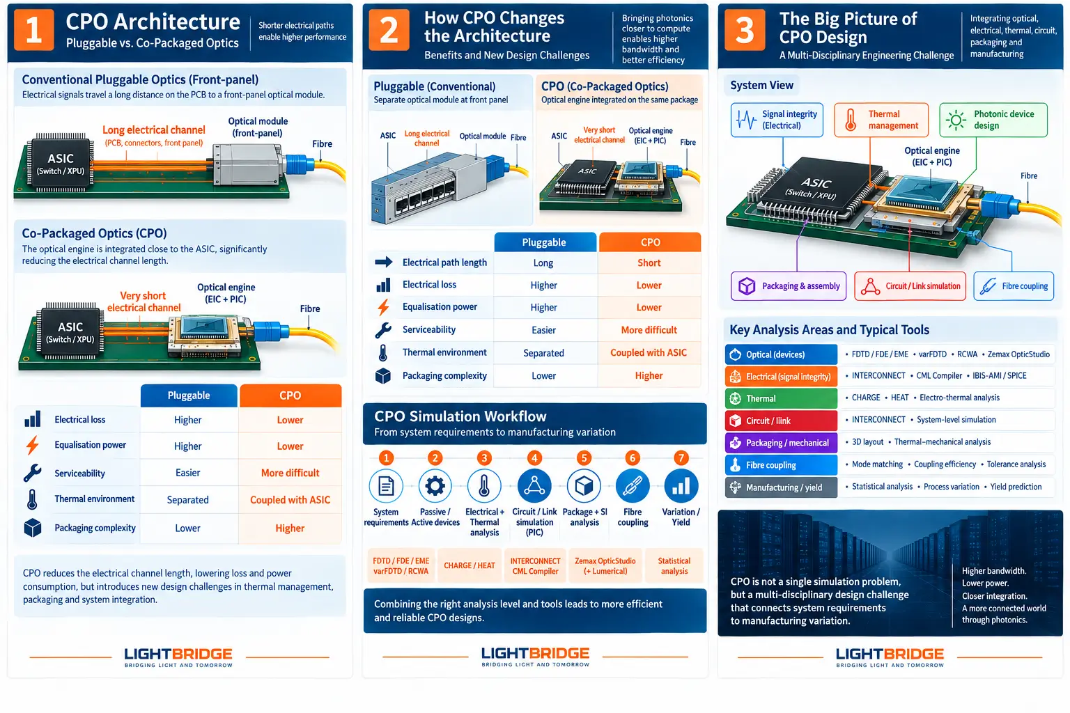
CPO is not one simulation problem. It is a hierarchy of coupled optical, electrical, thermal, circuit, packaging and manufacturing problems, organised below by the engineering question rather than by the solver.
What modes does this cross-section support? What is the insertion loss? How much does the response move if the geometry shifts a few nanometres? What is the wavelength dependence, and is there crosstalk into the neighbouring channel?
Different design questions require different simulation methods. FDE is well suited to calculating effective index, group index, dispersion, bend loss and mode overlap from a waveguide cross-section. Long adiabatic tapers, spot-size converters and MMIs are better handled with EME. Its cells require a cross-section that remains invariant along the propagation direction, and each solve considers one wavelength at a time. Once the modes have been calculated, however, the device length can be swept again without recomputing them, which makes taper optimisation practical. Problems involving grating couplers, strong scattering, back-reflection or significant out-of-plane behaviour generally call for 3D FDTD. Planar circuits extending a few hundred microns and containing rings or MZIs can often be simulated more efficiently with varFDTD, provided that coupling between vertical slab modes remains weak. It delivers a time-domain response at close to 2D computational cost. Applying full 3D FDTD to every passive device rarely improves the engineering decision enough to justify the additional simulation time.
An optical-only analysis cannot design a modulator. The physical chain is: applied bias changes the carrier distribution, the carrier distribution changes refractive index and absorption, the index change alters the optical mode response, and that determines modulation depth, bandwidth and drive voltage.
So the workflow crosses domains. CHARGE solves Poisson’s equation and the drift-diffusion equations self-consistently to give carrier distribution and junction capacitance against bias. That distribution is converted to an index perturbation — in Lumerical this handoff is an explicit object, with Soref-Bennett and Drude models available — and passed to an optical solve for effective index change and loss as a function of voltage. The figure of merit that comes out, VπLπ, is what the circuit level needs. For a ring modulator the practical order is FDTD for the coupling region, FDE for the passive bend, CHARGE for the active region, FDE again for the voltage-dependent active waveguide, then circuit simulation to assemble it.
Same structure, opposite direction: how the incident field distributes in the absorbing layer, and how the carriers it generates become an electrical response. For a Ge-on-Si detector the standard route is FDTD to obtain the spatial optical generation rate, then CHARGE with that rate as a source term in the continuity equations, giving responsivity, dark current and bandwidth. Not every detector workflow looks like this — in uni-travelling-carrier and avalanche devices the limiting mechanism differs, so the quantity worth computing differs too.
This is where CPO stops being an abstraction. A liquid-cooled 51.2 Tb/s CPO package has been characterised in both simulation and measurement with a 750 W switch ASIC and eight optical engines at 64 W each. The measured result: 98.3 °C at the switch junction and 35.1 °C at the hottest optical module. The same work states a maximum permissible module-to-module temperature difference of 4 °C (Wu et al., Front. Optoelectron., 2025).
Four degrees sounds generous until you convert it. A microring resonance moves roughly 0.1 nm per °C. On a WDM grid with 100–200 GHz spacing — 0.8 to 1.6 nm in the C band — a few degrees of gradient is a meaningful fraction of the channel spacing. The same physics sets the tuning cost, at around 39 mW for a π phase shift in a measured microring modulator, and in an engine with many rings that adds up.
The consequence is that package temperature becomes an input to photonic circuit performance, not a separate reliability question. HEAT solves conduction and Joule self-heating and can produce a thermal coupling matrix between heaters that the circuit simulator consumes directly. At package scale, a documented workflow computes the temperature field in Icepak, exports it as a map on the wafer coordinates, places the WDM circuit on that map, and runs temperature-sensitive compact models to get per-channel eye diagrams and BER. The thermal solver is not a downstream check; it feeds the link budget.
Correct device simulations do not tell you whether the link closes. The progression is device simulation → compact model extraction → PIC or transceiver circuit → wavelength response → eye diagram, BER, link margin.
Lumerical INTERCONNECT covers this with frequency-domain S-parameter analysis and two time-domain modes, and it is where the interesting failures show up: crosstalk as you add WDM channels, eye closure from a modulator whose extinction ratio looked acceptable in isolation, penalties from a filter that drifted. Getting device results into that environment is what CML Compiler is for, and when statistical data is supplied the models it builds support corner and Monte Carlo analysis.
The value of this stage is not verification but deciding device specifications. When the link misses its target, whether to spend the margin on modulator extinction ratio, coupling loss or channel spacing is a circuit-level judgement — and cheaper to make before the mask than after.
Short channels still need analysis; in some respects more, because impedance discontinuities and parasitics are a larger fraction of a small budget. The things that bite are interposer and RDL impedance and reflections, parasitic RLC between driver and modulator, crosstalk between densely packed high-speed channels, and high-frequency loss through TSVs, microbumps and BGA transitions.
The published CPO examples here are instructive: extract S-parameters for the interposer signal path with 3D electromagnetic simulation, bring them into the driver and photonic circuit simulations, and look at the eye at the transmitter, in the optical channel and at the receiver. In one documented case, adding the RF interconnect parasitics closes the eye almost completely.
This is the least glamorous part of CPO and the part most likely to determine yield. Edge couplers take light in through the facet and give broad bandwidth and low loss — a foundry-standard edge coupler measured around 1.5 dB per facet against a 3 µm mode-field-diameter lensed fibre. Grating couplers take light in through the surface, which makes wafer-level test possible, but the same comparison measured about 3 dB with a 1 dB bandwidth of only around 30 nm (Ranno et al., Photonics Res., 2024). Neither is simply better; loss and bandwidth are being traded for testability and assembly flow.
The real difficulty is the scale gap. A silicon waveguide mode is sub-micron to micron, a single-mode fibre mode is about 10 µm, and the fibre cladding is 125 µm. That last number constrains the package: attach fibres directly and the pitch cannot go below about 127 µm, which caps you at roughly eight fibres per millimetre of chip edge. Meanwhile the placement accuracy of high-throughput production pick-and-place equipment sits near 3 µm. Your coupler’s alignment tolerance therefore decides which assembly equipment — and which unit cost — you are allowed to use.
Spanning that gap means spanning two simulation domains. The waveguide mode belongs to FDE and FDTD; the microlens, the fibre geometry and the misalignment budget belong to ray and physical optics propagation in Zemax OpticStudio. The two exchange beam data as ZBF files, and there is a documented CPO example that solves a microlens-assisted edge coupler as FDE → OpticStudio physical optics propagation, including misalignment, → FDTD → EME. That chain puts a number on the decision to add a microlens to relax alignment tolerance, instead of arguing about it.
Nominal simulation is the starting point, not the deliverable. A 1 nm waveguide-width error shifts a filter wavelength by about 0.9 nm, and thickness variation is roughly twice as strong (Bogaerts et al., IEEE JSTQE, 2019). Wafer-scale characterisation also shows that 1,200 nm-wide waveguides vary substantially less than 480 nm ones — a design choice available to you, not just a fab property.
Variation shows up twice: as channels landing off their assigned grid, and as the thermal tuning power needed to pull them back. So the last step of a CPO design is distributional. Supply the compact models with statistical parameters and correlation lengths, run Monte Carlo, and read yield off the distribution of extinction ratio, link loss and tuning power. Because a CPO engine has many nominally identical devices spread over millimetres, layout-aware approaches that import physical coordinates so the spatial correlation reflects actual placement matter here too.
Laid out as one sequence, the above becomes: system requirement → passive and active device analysis → electrical and thermal analysis → compact model extraction → PIC and link simulation → package and signal-integrity evaluation → fibre coupling → process variation and yield. No project should follow that order rigidly. If the foundry PDK already has the devices, starting at the link level is faster. If thermal gradient is known to dominate, put thermal first and let it constrain the device specifications. Debugging an existing design usually means walking the sequence backwards from the measured symptom.
The most common way a CPO simulation effort goes wrong is starting from “which tool should we use”. Inverting that saves weeks.
| If the question is… | The method is… | And you get… |
|---|---|---|
| Guided modes, n_eff, dispersion, bend loss | FDE | The basis for circuit models and coupling design |
| Length of a taper, MMI or spot-size converter | EME | S-parameters and an optimal length |
| Grating coupling, scattering, out-of-plane behaviour | 3D FDTD | Coupling efficiency, wavelength and polarisation response |
| Periodic or multilayer structures | RCWA | Diffraction efficiency (not for non-periodic transverse variation) |
| Carrier transport, junction capacitance | CHARGE | The input to index change and bandwidth |
| Temperature field, thermal crosstalk | HEAT | Resonance shift and tuning power |
| Whole-link eye, BER, yield | INTERCONNECT | Requirements to push back onto the devices |
| Package optics and fibre alignment tolerance | Zemax OpticStudio with Lumerical | Assembly tolerance and equipment implications |
Once the question is stated properly, the method is usually obvious.
Weeks of 3D FDTD on passive components will not save a link whose thermal gradient was underestimated, and a clean thermal and circuit model will not reach production if the coupler’s alignment tolerance is tighter than the assembly equipment can hold. The difficulty in CPO is not any single device — it is deciding which question belongs at which level.
Of the methods named above, FDE, EME and varFDTD ship in Lumerical MODE, while CHARGE and HEAT are part of Lumerical Multiphysics. LightBridge supplies and supports Ansys Lumerical and Zemax OpticStudio, and our PIC design workflow, silicon photonics and optical communications pages set out how device, circuit and yield analysis fit together. For projects heading towards fabrication, we also advise on foundry selection and design data preparation, including MPW runs — within the scope of the target foundry’s PDK and design rules.
The first decision on a CPO project is not the software stack. It is which question you need answered now.
Our engineers can advise on building a design flow for your application, and on validating an analysis model, from practical experience.